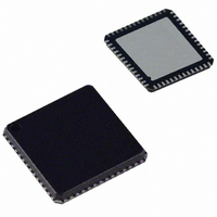
AD9995KCP Analog Devices Inc, AD9995KCP Datasheet - Page 30

AD9995KCP
Manufacturer Part Number
AD9995KCP
Description
IC CCD SIGNAL PROCESSOR 56-LFCSP
Manufacturer
Analog Devices Inc
Type
CCD Signal Processor, 12-Bitr
Datasheet
1.AD9995KCPZRL.pdf
(60 pages)
Specifications of AD9995KCP
Rohs Status
RoHS non-compliant
Input Type
Logic
Output Type
Logic
Interface
3-Wire Serial
Current - Supply
30mA
Mounting Type
Surface Mount
Package / Case
56-LFCSP
Analog Front End Type
CCD
Analog Front End Category
Video
Interface Type
Serial (3-Wire)
Input Voltage Range
0.5V
Operating Supply Voltage (min)
2.7V
Operating Supply Voltage (typ)
3V
Operating Supply Voltage (max)
3.6V
Resolution
12b
Number Of Adc's
1
Power Supply Type
Analog/Digital
Operating Temp Range
-20C to 85C
Operating Temperature Classification
Commercial
Mounting
Surface Mount
Pin Count
56
Package Type
LFCSP EP
Number Of Channels
1
Lead Free Status / RoHS Status
Not Compliant
Available stocks
Company
Part Number
Manufacturer
Quantity
Price
Company:
Part Number:
AD9995KCP
Manufacturer:
ADI
Quantity:
148
Company:
Part Number:
AD9995KCPZ
Manufacturer:
ADI
Quantity:
24
Company:
Part Number:
AD9995KCPZRL7
Manufacturer:
SANYO
Quantity:
1 170
MECHANICAL
EXPOSURE AND READOUT EXAMPLE
AD9995
1. Write to the READOUT register (Addr. 0x61) to specify
2. VD/HD falling edge will update the serial writes from 1.
3. If VSUB mode = 0 (Addr. 0x67), VSUB output turns on at
4. STROBE output turns on and off at the location specified
SHUTTER
STROBE
WRITES
SERIAL
SUBCK
MSHUT
Write to the EXPOSURE register (Addr. 0x62) to specify
Write to the TRIGGER register (Addr. 0x60) to enable the
Write to the MODE register (Addr. 0x1B) to configure the
the number of fields to further suppress SUBCK while the
CCD data is read out. In this example, READOUT = 3.
the number of fields to suppress SUBCK and VSG outputs
during exposure. In this example, EXPOSURE = 1.
STROBE, MSHUT, and VSUB signals, and to start the
exposure/readout operation. To trigger all of these events (as
in Figure 32), set the register TRIGGER = 31. Readout will
automatically occur after the exposure period is finished.
next five fields. The first two fields during exposure are the
same as the current draft mode fields, and the following
three fields are the still frame readout fields. The registers
for the Draft mode field and the three readout fields have
already been programmed.
the line specified in the VSUBON register (Addr. 0x68).
in the STROBEON and OFF registers (Addr. 0x6E to
Addr. 0x71).
VSUB
CCD
VSG
OUT
VD
Figure 32. Example of Exposure and Still Image Readout Using Shutter Signals and Mode Register
1
DRAFT IMAGE
2
DRAFT IMAGE
3
MODE 0
4
t
EXP
OPEN
5
MODE 1
CLOSED
6
STILL IMAGE 1ST FIELD
–30–
10. VD/HD falling edge will update the serial write from 9.
5. MSHUT output turns off at the location specified in the
6. The next VD falling edge will automatically start the first
7. The next VD falling edge will automatically start the second
8. The next VD falling edge will automatically start the third
9. Write to the MODE register to reconfigure the single Draft
7
STILL IMAGE READOUT
Write to the MSHUTON register (Addr. 0x6A) to open the
VSG outputs return to Draft mode timing.
VSUB output returns to the off position (inactive).
MSHUTOFF registers (Addr. 0x6B and 0x6C).
readout field.
readout field.
readout field.
mode field timing.
mechanical shutter.
SUBCK output resumes operation.
MSHUT output returns to the on position (active or open).
STILL IMAGE 2ND FIELD
8
STILL IMAGE 3RD FIELD
9
10
10
10
10
OPEN
DRAFT IMAGE
REV. 0


