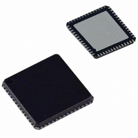
AD9995KCP Analog Devices Inc, AD9995KCP Datasheet - Page 23

AD9995KCP
Manufacturer Part Number
AD9995KCP
Description
IC CCD SIGNAL PROCESSOR 56-LFCSP
Manufacturer
Analog Devices Inc
Type
CCD Signal Processor, 12-Bitr
Datasheet
1.AD9995KCPZRL.pdf
(60 pages)
Specifications of AD9995KCP
Rohs Status
RoHS non-compliant
Input Type
Logic
Output Type
Logic
Interface
3-Wire Serial
Current - Supply
30mA
Mounting Type
Surface Mount
Package / Case
56-LFCSP
Analog Front End Type
CCD
Analog Front End Category
Video
Interface Type
Serial (3-Wire)
Input Voltage Range
0.5V
Operating Supply Voltage (min)
2.7V
Operating Supply Voltage (typ)
3V
Operating Supply Voltage (max)
3.6V
Resolution
12b
Number Of Adc's
1
Power Supply Type
Analog/Digital
Operating Temp Range
-20C to 85C
Operating Temperature Classification
Commercial
Mounting
Surface Mount
Pin Count
56
Package Type
LFCSP EP
Number Of Channels
1
Lead Free Status / RoHS Status
Not Compliant
Available stocks
Company
Part Number
Manufacturer
Quantity
Price
Company:
Part Number:
AD9995KCP
Manufacturer:
ADI
Quantity:
148
Company:
Part Number:
AD9995KCPZ
Manufacturer:
ADI
Quantity:
24
Company:
Part Number:
AD9995KCPZRL7
Manufacturer:
SANYO
Quantity:
1 170
MODE Register
The MODE register is a single register that selects the field tim-
ing of the AD9995. Typically, all of the field, V-sequence, and
V-pattern group information is programmed into the AD9995
at startup. During operation, the MODE register allows the user
to select any combination of field timing to meet the current
requirements of the system. The advantage of using the MODE
register in conjunction with preprogrammed timing is that it
greatly reduces the system programming requirements during
camera operation. Only a few register writes are required when
the camera operating mode is changed, rather than having to
write in all of the vertical timing information with each camera
mode change.
A basic still camera application might require five different
fields of vertical timing: one for draft mode operation, one for
autofocusing, and three for still image readout. All of the reg-
ister timing information for the five fields would be loaded at
REV. 0
Total Number of
D23
Fields to Use.
1 = 1st Field Only 5 = Field 5
7 = All 7 Fields
0 = Invalid
22
21
20
7th Field
0 = Field 0
6, 7 = Invalid
19
EXAMPLE 1:
TOTAL FIELDS = 3, 1ST FIELD = FIELD 0, 2ND FIELD = FIELD 1, 3RD FIELD = FIELD 2
MODE REGISTER CONTENTS = 0x600088
EXAMPLE 3:
TOTAL FIELDS = 4, 1ST FIELD = FIELD 5, 2ND FIELD = FIELD 1, 3RD FIELD = FIELD 4, 4TH FIELD = FIELD 2
MODE REGISTER CONTENTS = 0x80050D
EXAMPLE 2:
TOTAL FIELDS = 2, 1ST FIELD = FIELD 3, 2ND FIELD = FIELD 4
MODE REGISTER CONTENTS = 0x400023
FIELD 0
FIELD 3
FIELD 5
18
Figure 24. Using the MODE Register to Select FieldTiming
Table X. MODE Register Data Bit Breakdown (D23 = MSB)
17
6th Field
0 = Field 0
5 = Field 5
6, 7 = Invalid
16
FIELD 1
FIELD 4
FIELD 1
15
14
5th Field
0 = Field 0
5 = Field 5
6, 7 = Invalid
FIELD 2
FIELD 4
13
–23–
12
startup. Then, during camera operation, the MODE register
would select which field timing would be active, depending on
how the camera was being used.
Table X shows how the MODE register bits are used. The three
MSBs, D23–D21, are used to specify how many total fields will
be used. Any value from 1 to 7 can be selected using these three
bits. The remaining register bits are divided into 3-bit sections to
select which of the six fields are used and in which order. Up to
seven fields may be used in a single MODE write. The AD9995
will start with the Field timing specified by the first Field bits,
and on the next VD will switch to the timing specified by the
second Field bits, and so on.
After completing the total number of fields specified in Bits
D23 to D21, the AD9995 will repeat by starting at the first
Field again. This will continue until a new write to the MODE
register occurs. Figure 24 shows example MODE register set-
tings for different field configurations.
11
4th Field
0 = Field 0
5 = Field 5
6, 7 = Invalid
FIELD 2
10
9
8
3rd Field
0 = Field 0
5 = Field 5
6, 7 = Invalid
7
6
5
2nd Field
0 = Field 0
5 = Field 5
6, 7 = Invalid
4
3
AD9995
2
1st Field
0 = Field 0
5 = Field 5
6, 7 = Invalid
1
D0


