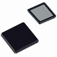
AD9995KCP Analog Devices Inc, AD9995KCP Datasheet - Page 19

AD9995KCP
Manufacturer Part Number
AD9995KCP
Description
IC CCD SIGNAL PROCESSOR 56-LFCSP
Manufacturer
Analog Devices Inc
Type
CCD Signal Processor, 12-Bitr
Datasheet
1.AD9995KCPZRL.pdf
(60 pages)
Specifications of AD9995KCP
Rohs Status
RoHS non-compliant
Input Type
Logic
Output Type
Logic
Interface
3-Wire Serial
Current - Supply
30mA
Mounting Type
Surface Mount
Package / Case
56-LFCSP
Analog Front End Type
CCD
Analog Front End Category
Video
Interface Type
Serial (3-Wire)
Input Voltage Range
0.5V
Operating Supply Voltage (min)
2.7V
Operating Supply Voltage (typ)
3V
Operating Supply Voltage (max)
3.6V
Resolution
12b
Number Of Adc's
1
Power Supply Type
Analog/Digital
Operating Temp Range
-20C to 85C
Operating Temperature Classification
Commercial
Mounting
Surface Mount
Pin Count
56
Package Type
LFCSP EP
Number Of Channels
1
Lead Free Status / RoHS Status
Not Compliant
Available stocks
Company
Part Number
Manufacturer
Quantity
Price
Company:
Part Number:
AD9995KCP
Manufacturer:
ADI
Quantity:
148
Company:
Part Number:
AD9995KCPZ
Manufacturer:
ADI
Quantity:
24
Company:
Part Number:
AD9995KCPZRL7
Manufacturer:
SANYO
Quantity:
1 170
Complete Field: Combining V-Sequences
After the V-sequences have been created, they are combined to
create different readout fields. A field consists of up to seven
different regions, and within each region a different V-sequence
can be selected. Figure 18 shows how the sequence change posi-
tions (SCP) designate the line boundary for each region, and
the VSEQSEL registers then select which V-sequence is used
during each region. Registers to control the VSG outputs are also
included in the Field registers.
Table VII summarizes the registers used to create the different
fields. Up to six different fields can be preprogrammed using all
of the Field registers.
The VEQSEL registers, one for each region, select which of the
10 V-sequences will be active during each region. The SWEEP
registers are used to enable SWEEP mode during any region.
The MULTI registers are used to enable Multiplier mode dur-
Register
VSEQSEL
SWEEP
MULTI
SCP
VDLEN
HDLAST
VPATSECOND
SGMASK
SGPATSEL
SGLINE1
SGLINE2
REV. 0
V1–V6
VSG
HD
VD
FIELD SETTINGS:
1. SEQUENCE CHANGE POSITIONS (SCP1–6) DEFINE EACH OF THE 7 REGIONS IN THE FIELD.
2. VSEQSEL0–6 SELECTS THE DESIRED V-SEQUENCE (0–9) FOR EACH REGION.
3. SGLINE1 REGISTER SELECTS WHICH HD LINE IN THE FIELD WILL CONTAIN THE SENSOR GATE PULSE(S).
Length
4b
1b
1b
12b
12b
12b
4b
6b
12b
12b
12b
VSEQSEL0
REGION 0
SCP 1
Range
0–9 V-Sequence #
High/Low
High/Low
0–4095 Line #
0–4095 # of Lines
0–4095 # of Pixels
0–9 V-Pattern Group #
High/Low, Each VSG
0–3 Pattern #, Each VSG
0–4095 Line #
0–4095 Line #
VSEQSEL1
VSEQSEL1
VSEQSEL1
VSEQSEL1
REGION 1
Figure 18. Complete Field Is Divided into Regions
SGLINE
SGLINE
SGLINE
SGLINE1
SCP 2
VSEQSEL2
REGION 2
Table VII. Field Registers
SCP 3
VSEQSEL3
REGION 3
VSG3 [2], VSG4 [3], VSG5 [4].
VSG2 [3:2], VSG3 [5:4], VSG4 [7:6], VSG5 [9:8].
Description
Selected V-Sequence for Each Region in the Field.
Enables Sweep Mode for Each Region, When Set High.
Enables Multiplier Mode for Each Region, When Set High.
Sequence Change Position for Each Region.
Total Number of Lines in Each Field.
Length in Pixels of the Last HD Line in Each Field.
Selected V-Pattern Group for Second Pattern Applied During VSG Line.
Set High to Mask Each Individual VSG Output. VSG1 [0], VSG2 [1],
Selects the VSG Pattern Number for Each VSG Output. VSG1 [1:0],
Selects the Line in the Field where the VSG Are Active.
Selects a Second Line in the Field to Repeat the VSG Signals.
–19–
ing any region. The SCP registers create the line boundaries for
each region. The VDLEN register specifies the total number of
lines in the field. The total number of pixels per line (HDLEN) is
specified in the V-sequence registers, but the HDLAST register
specifies the number of pixels in the last line of the field. The
VPATSECOND register is used to add a second V-pattern group
to the V1–6 outputs during the sensor gate (VSG) line.
The SGMASK register is used to enable or disable each indi-
vidual VSG output. There is a single bit for each VSG output;
setting the bit high will mask the output, setting it low will enable
the output. The SGPAT register assigns one of the four different
SG patterns to each VSG output. The individual SG patterns are
created separately using the SG pattern registers. The SGLINE1
register specifies which line in the field will contain the VSG out-
puts. The optional SGLINE2 register allows the same VSG pulses
to be repeated on a different line.
SCP 4
VSEQSEL4
REGION 4
SCP 5
VSEQSEL5
REGION 5
SCP 6
VSEQSEL6
REGION 6
AD9995


