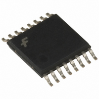
FIN1049MTC Fairchild Semiconductor, FIN1049MTC Datasheet

FIN1049MTC
Specifications of FIN1049MTC
Available stocks
Related parts for FIN1049MTC
FIN1049MTC Summary of contents
Page 1
... Industrial Operating Temperature Range: -40°C to +85°C Ordering Information Operating Part Number Temperature Range FIN1049MTCX -40 to +85°C For Fairchild’s definition of Eco Status, please visit: http://www.fairchildsemi.com/company/green/rohs_green.html. © 2003 Fairchild Semiconductor Corporation FIN1049 • Rev. 1.0.2 Description This dual driver-receiver is designed for high-speed interconnects utilizing Low Voltage Differential Signaling (LVDS) technology ...
Page 2
... H=HIGH Logic Level L=LOW Logic Level or OPEN X=Don't Care Z=High Impedance Note: 1. Any unused receiver Inputs should be left open. © 2003 Fairchild Semiconductor Corporation FIN1049 • Rev. 1.0.2 Functional Diagram Non-Inverting LVDS Inputs Inverting LVDS Inputs Non-Inverting Driver Outputs Inverting Driver Outputs ...
Page 3
... Fairchild does not recommend exceeding them or designing to Absolute Maximum Ratings. Symbol V Supply Voltage Magnitude of Differential Voltage ID T Operating Temperature A © 2003 Fairchild Semiconductor Corporation FIN1049 • Rev. 1.0.2 Parameter Parameter 3 Min. Max. -0.5 +4.6 -0.5 +4.6 -0.5 +4.6 ...
Page 4
... C Input Capacitance INT Note: 2. Both driver and receiver inputs are static. All LVDS outputs have 100Ω load. None of the outputs have any lumped capacitive load. © 2003 Fairchild Semiconductor Corporation FIN1049 • Rev. 1.0.2 Conditions , See Figure 3 and Table 1 IN1+ ...
Page 5
... MAXD cycle=45% / 55%, V > 250mV, all channels switch generator input conditions: t MAXT criteria: duty cycle=45% / 55%, V © 2003 Fairchild Semiconductor Corporation FIN1049 • Rev. 1.0.2 Conditions | (3) See Figure 7, Figure 8 (5) See Figure 5 Measured from 20% to 80% Signal V =200mV; ID ...
Page 6
... V IA 1.25 1. 0.1 CC 0.1 0.0 1.75 0. 1.1 CC 1.1 0.0 Note: 10. R =100Ω. L © 2003 Fairchild Semiconductor Corporation FIN1049 • Rev. 1.0.2 Resulting Differential Input Voltage (mV 1.15 100 1.25 -100 V - 0.1 100 CC V -100 CC 0.0 100 0.1 -100 0.65 1100 1.75 ...
Page 7
... Required Specifications and Test Diagrams Figure 5. LVDS Output Propagation Delay and Transition Time Test Circuit Notes: 11 =100Ω =50Ω and C =15pF distributed Figure 6. LVTTL Input to LVDS Output AC Waveform © 2003 Fairchild Semiconductor Corporation FIN1049 • Rev. 1.0.2 (Continued) 7 www.fairchildsemi.com ...
Page 8
... Figure 7. LVDS Output Enable / Disable Delay Test Circuit Notes: 13 =100Ω =50Ω and C =15pF distributed 15. R1=1000Ω, R =950Ω. S 16. V =2.4V. TST Figure 8. LVDS Output Enable / Disable Timing Waveforms © 2003 Fairchild Semiconductor Corporation FIN1049 • Rev. 1.0.2 (Continued) 8 www.fairchildsemi.com ...
Page 9
... Figure 9. LVTTL Output Propagation Delay and Transition Time Test Circuit Notes: 17 =50Ω and C =15pF distributed 18. R =100Ω and R =950Ω Figure 10. LVDS Input to LVTTL Output Propagation Delay and Transition Time Waveforms © 2003 Fairchild Semiconductor Corporation FIN1049 • Rev. 1.0.2 (Continued) 9 www.fairchildsemi.com ...
Page 10
... Required Specifications and Test Diagrams Figure 11. LVTTL Output Enable / Disable Test Circuit Notes: 19 =50Ω and C =15pF distributed 20. R =100Ω, R1=1000Ω, and R L Figure 12. LVTTL Output Enable / Disable Timing Waveforms © 2003 Fairchild Semiconductor Corporation FIN1049 • Rev. 1.0.2 (Continued) =950Ω www.fairchildsemi.com ...
Page 11
... Package drawings are provided as a service to customers considering Fairchild components. Drawings may change in any manner without notice. Please note the revision and/or date on the drawing and contact a Fairchild Semiconductor representative to verify or obtain the most recent revision. Package specifications do not expand the terms of Fairchild’s worldwide terms and conditions, specifically the warranty therein, which covers Fairchild products. Always visit Fairchild Semiconductor’ ...
Page 12
... Fairchild Semiconductor Corporation FIN1049 • Rev. 1.0.2 12 www.fairchildsemi.com ...


