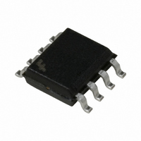
FIN1017M Fairchild Semiconductor, FIN1017M Datasheet - Page 4

FIN1017M
Manufacturer Part Number
FIN1017M
Description
IC DRIVER 3.3V LVDS HS 8SOIC
Manufacturer
Fairchild Semiconductor
Type
Driverr
Datasheet
1.FIN1017MX.pdf
(11 pages)
Specifications of FIN1017M
Number Of Drivers/receivers
1/0
Protocol
LVDS
Voltage - Supply
3 V ~ 3.6 V
Mounting Type
Surface Mount
Package / Case
8-SOIC (3.9mm Width)
Lead Free Status / RoHS Status
Lead free / RoHS Compliant
Available stocks
Company
Part Number
Manufacturer
Quantity
Price
Company:
Part Number:
FIN1017MX
Manufacturer:
VISHAY
Quantity:
32 600
Part Number:
FIN1017MX
Manufacturer:
FAIRCHILD/仙童
Quantity:
20 000
© 2001 Fairchild Semiconductor Corporation
FIN1017 • Rev. 1.0.3
DC Electrical Characteristics
Over-supply voltage and operating temperature ranges, unless otherwise specified. All typical values are at T
25°C and with V
Symbol
AC Electrical Characteristics
Over-supply voltage and operating temperature ranges, unless otherwise specified. All typical values are at T
25°C and with V
Note:
2.
Symbol
ΔV
ΔV
I
C
t
V
I(OFF)
t
t
t
t
t
V
I
SK(PP)
C
V
V
I
V
I
PLHD
PHLD
SK(P)
OFF
TLHD
THLD
I
OS
CC
OUT
IN
OD
OS
IH
t
devices switching in the same direction (either LOW-to-HIGH or HIGH-to-LOW) when both devices operate with
the same supply voltage, same temperature, and have identical test circuits.
IL
IK
IN
OD
OS
SK(PP)
Output Differential Voltage
V
Differential LOW-to-HIGH
Offset Voltage
Offset Magnitude Change from
Differential LOW-to-HIGH
Power-Off Output Current
Short-Circuit Output Current
Input HIGH Voltage
Input LOW Voltage
Input Current
Power-Off Input Current
Input Clamp Voltage
Power Supply Current
Input Capacitance
Output Capacitance
is the magnitude of the difference in propagation delay times between any specified terminals of two
Differential Propagation Delay, LOW-to-HIGH
Differential Propagation Delay, HIGH-to-LOW
Differential Output Rise Time (20% to 80%)
Differential Output Fall Time (80% to 20%)
Pulse Skew |t
Part-to-Part Skew
OD
Magnitude Change from
CC
CC
= 3.3V.
= 3.3V.
Parameter
PLH
- t
(2)
Parameter
PHL
|
R
V
V
V
V
V
I
No Load, V
R
IK
CC
OUT
OD
IN
CC
L
L
= -18mA
= 100 Ω, See Figure 3
= 100Ω, V
= 0V or V
= 0V, V
= 0V, V
= 0V
= 0V
4
Conditions
IN
OUT
IN
CC
IN
= 0V or V
= 0V or 3.6V
R
see Figure 4 and Figure 5
= 0V or 3.6V
= 0V or V
L
= 100Ω, C
Test Conditions
CC
CC
L
= 10pF,
1.125
Min.
GND
250
-1.5
2
1.250
Typ.
350
4
6
Min. Max. Units
0.5
0.5
0.4
0.4
Max.
1.375
450
±20
V
±20
±20
0.8
25
25
±8
10
-8
8
CC
1.5
1.5
1.0
1.0
0.5
1.0
www.fairchildsemi.com
Units
mV
mV
mV
mA
mA
mA
mA
mA
mA
pF
pF
V
V
V
V
ns
ns
ns
ns
ns
ns
A
A
=
=


