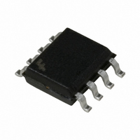
FIN1018M Fairchild Semiconductor, FIN1018M Datasheet - Page 2

FIN1018M
Manufacturer Part Number
FIN1018M
Description
RECEIVER 3.3V LVDS HS 8-SOIC
Manufacturer
Fairchild Semiconductor
Type
Receiverr
Datasheet
1.FIN1018K8X.pdf
(8 pages)
Specifications of FIN1018M
Number Of Drivers/receivers
0/1
Protocol
LVDS
Voltage - Supply
3 V ~ 3.6 V
Mounting Type
Surface Mount
Package / Case
8-SOIC (3.9mm Width)
Logic Family
FIN10
Logic Type
High Speed Differential Receiver
Supply Voltage (max)
3.6 V
Supply Voltage (min)
3 V
Maximum Operating Temperature
+ 85 C
Mounting Style
SMD/SMT
Data Rate
400 Mbps
Interface
EIA/TIA-644
Minimum Operating Temperature
- 40 C
Number Of Lines (input / Output)
1 / 1
Supply Current
7 mA
Lead Free Status / RoHS Status
Lead free / RoHS Compliant
Available stocks
Company
Part Number
Manufacturer
Quantity
Price
Company:
Part Number:
FIN1018MX
Manufacturer:
FSC
Quantity:
5 122
www.fairchildsemi.com
t
t
t
t
t
t
V
V
I
I
V
V
V
I
C
C
PLH
PHL
TLH
THL
SK(P)
SK(PP)
Absolute Maximum Ratings
DC Electrical Characteristics
Over supply voltage and operating temperature ranges, unless otherwise specified
IN
I(OFF)
CC
Note 2: All typical values are at T
AC Electrical Characteristics
Over supply voltage and operating temperature ranges, unless otherwise specified
Note 3: All typical values are at T
Note 4: t
(either LOW-to-HIGH or HIGH-to-LOW) when both devices operate with the same supply voltage, same temperature, and have identical test circuits.
Supply Voltage (V
DC Input Voltage (R
DC Output Voltage (D
DC Output Current (I
Storage Temperature Range (T
Max Junction Temperature (T
Lead Temperature (T
ESD (Human Body Model)
ESD (Bus Pins R
ESD (Machine Model)
Symbol
TH
TL
OH
OL
IK
IN
OUT
Symbol
(Soldering, 10 seconds)
SK(PP)
Propagation Delay LOW-to-HIGH
Propagation Delay HIGH-to-LOW
Output Rise Time (20% to 80%)
Output Fall Time (80% to 20%)
Pulse Skew |t
Part-to-Part Skew (Note 4)
Differential Input Threshold HIGH
Differential Input Threshold LOW
Input Current
Power-OFF Input Current
Output HIGH Voltage
Output LOW Voltage
Input Clamp Voltage
Power Supply Current
Input Capacitance
Output Capacitance
is the magnitude of the difference in propagation delay times between any specified terminals of two devices switching in the same direction
IN
CC
IN
/R
)
O
Parameter
L
PLH
OUT
)
)
IN
, R
Parameter
- t
)
to GND)
A
A
IN
PHL
25 C and with V
25 C and with V
)
J
|
)
STG
)
CC
CC
See Figure 1 and Table 1
See Figure 1 and Table 1
V
V
I
I
I
I
I
Inputs Open, (R
or (R
OH
OH
OH
OL
IK
65 C to 150 C
IN
CC
3.3V.
3.3V.
0.5V to 4.6V
0.5V to 4.7V
(Note 1)
IN
8 mA
0V or V
100 A
0.5V to 6V
18 mA
0V, V
|V
See Figure 1 and Figure 2
100 A
8 mA
ID
1.4V and R
|
IN
16 mA
6500V
9500V
150 C
260 C
Test Conditions
CC
300V
400 mV, C
IN
0V or 3.6V
Test Conditions
1V and R
2
IN
Recommended Operating
Conditions
Note 1: The “Absolute Maximum Ratings”: are those values beyond which
damage to the device may occur. The databook specifications should be
met, without exception, to ensure that the system design is reliable over its
power supply, temperature and output/input loading variables. Fairchild
does not recommend operation of circuits outside databook specification.
L
Supply Voltage (V
Input Voltage (V
Magnitude of Differential Voltage
Common-mode Input Voltage (V
Operating Temperature (T
1V)
(|V
10 pF
ID
IN
|)
1.4V),
IN
V
CC
)
CC
Min
2.4
100
Min
)
1.5
0.9
0.9
0.2
A
)
(Note 2)
(Note 3)
Typ
Typ
0.5
0.5
4
6
IC
)
Max
100
0.2
0.5
Max
2.5
2.5
0.4
1.0
20
20
7
0.05V to 2.35V
100mV to V
40 C to 85 C
3.0V to 3.6V
0 to V
Units
Units
mV
mV
mA
pF
pF
V
V
V
V
V
ns
ns
ns
ns
ns
ns
A
A
CC
CC


