Ordering Information
* Same as SOT-89. Product supplied on 2000 piece carrier tape reels.
†
11/12/01
Supertex Inc. does not recommend the use of its products in life support applications and will not knowingly sell its products for use in such applications unless it receives an adequate "products liability
indemnification insurance agreement." Supertex does not assume responsibility for use of devices described and limits its liability to the replacement of devices determined to be defective due to
workmanship. No responsibility is assumed for possible omissions or inaccuracies. Circuitry and specifications are subject to change without notice. For the latest product specifications, refer to the
Supertex website: http://www.supertex.com. For complete liability information on all Supertex products, refer to the most current databook or to the Legal/Disclaimer page on the Supertex website.
Features
❏ Free from secondary breakdown
❏ Low power drive requirement
❏ Ease of paralleling
❏ Low C
❏ Excellent thermal stability
❏ Integral Source-Drain diode
❏ High input impedance and high gain
❏ Complementary N- and P-channel devices
Applications
❏ Motor controls
❏ Converters
❏ Amplifiers
❏ Switches
❏ Power supply circuits
❏ Drivers (relays, hammers, solenoids, lamps,
Absolute Maximum Ratings
Drain-to-Source Voltage
Drain-to-Gate Voltage
Gate-to-Source Voltage
Operating and Storage Temperature
Soldering Temperature*
* Distance of 1.6 mm from case for 10 seconds.
MIL visual screening available
Where ❋ = 2-week alpha date code
Product marking for TO-243AA:
memories, displays, bipolar transistors, etc.)
BV
BV
50V
DSS
DGS
ISS
and fast switching speeds
/
VN2L❋
R
(max)
0.3Ω
DS(ON)
N-Channel Enhancement-Mode
Vertical DMOS FETs
-55°C to +150°C
V
(max)
2.4V
GS(th)
BV
300°C
BV
± 20V
DGS
DSS
VN3205N3
1
TO-92
Advanced DMOS Technology
These enhancement-mode (normally-off) transistors utilize a
vertical DMOS structure and Supertex’s well-proven silicon-gate
manufacturing process. This combination produces devices with
the power handling capabilities of bipolar transistors and with the
high input impedance and positive temperature coefficient
inherent in MOS devices. Characteristic of all MOS structures,
these devices are free from thermal runaway and thermally-
induced secondary breakdown.
Supertex’s vertical DMOS FETs are ideally suited to a wide range
of switching and amplifying applications where high breakdown
voltage, high input impedance, low input capacitance, and fast
switching speeds are desired.
Package Options
Note: See Package Outline section for dimensions.
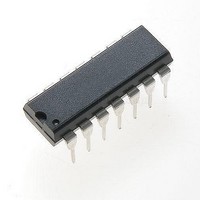
14-Pin P-DIP
TO-92
VN3205N6
S G D
Order Number / Package
NC
G
G
D
D
S
S
1
1
1
2
2
2
2
3
4
5
6
7
1
14-pin DIP
top view
TO-243AA*
VN3205N8
13
12
11
10
9
8
14
G
TO-243AA
(SOT-89)
D
VN3205
S
D
G
S
NC
S
G
D
VN3205ND
4
3
4
4
3
3
Die
D
†