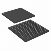
DS26518GN+ Maxim Integrated Products, DS26518GN+ Datasheet - Page 6

DS26518GN+
Manufacturer Part Number
DS26518GN+
Description
IC TXRX T1/E1/J1 8PORT 256-CSBGA
Manufacturer
Maxim Integrated Products
Type
Transceiverr
Specifications of DS26518GN+
Number Of Drivers/receivers
8/8
Protocol
T1/E1/J1
Voltage - Supply
3.135 V ~ 3.465 V
Mounting Type
Surface Mount
Package / Case
256-CSBGA
Lead Free Status / RoHS Status
Lead free / RoHS Compliant
- Current page: 6 of 286
- Download datasheet (2Mb)
DS26518 8-Port T1/E1/J1 Transceiver
Figure 11-18. E1 Receive-Side Boundary Timing (Elastic Store Disabled) ............................................................ 255
Figure 11-19. E1 Receive-Side 1.544MHz Boundary Timing (Elastic Store Enabled)............................................ 256
Figure 11-20. E1 Receive-Side 2.048MHz Boundary Timing (Elastic Store Enabled)............................................ 256
Figure 11-21. E1 Receive-Side Interleave Bus Operation—BYTE Mode ............................................................... 257
Figure 11-22. E1 Receive-Side Interleave Bus Operation—FRAME Mode ............................................................ 258
Figure 11-23. E1 Receive-Side RCHCLKn Gapped Mode During Channel 1 ........................................................ 258
Figure 11-24. E1 Transmit-Side Timing................................................................................................................... 259
Figure 11-25. E1 Transmit-Side Boundary Timing (Elastic Store Disabled) ........................................................... 259
Figure 11-26. E1 Transmit-Side 1.544MHz Boundary Timing (Elastic Store Enabled)........................................... 260
Figure 11-27. E1 Transmit-Side 2.048MHz Boundary Timing (Elastic Store Enabled)........................................... 260
Figure 11-28. E1 Transmit-Side Interleave Bus Operation—BYTE Mode .............................................................. 261
Figure 11-29. E1 Transmit-Side Interleave Bus Operation—FRAME Mode ........................................................... 262
Figure 11-30. E1 G.802 Timing ............................................................................................................................... 263
Figure 11-31. E1 Transmit-Side TCHCLKn Gapped Mode During Channel 1 ........................................................ 263
Figure 13-1. SPI Interface Timing Diagram ............................................................................................................. 267
Figure 13-2. Intel Bus Read Timing (BTS = 0) ........................................................................................................ 269
Figure 13-3. Intel Bus Write Timing (BTS = 0)......................................................................................................... 269
Figure 13-4. Motorola Bus Read Timing (BTS = 1) ................................................................................................. 270
Figure 13-5 Motorola Bus Write Timing (BTS = 1) .................................................................................................. 270
Figure 13-6. Receive Framer Timing—Backplane (T1 Mode)................................................................................. 272
Figure 13-7. Receive-Side Timing—Elastic Store Enabled (T1 Mode) ................................................................... 273
Figure 13-8. Receive Framer Timing—Line Side .................................................................................................... 273
Figure 13-9. Transmit Formatter Timing—Backplane ............................................................................................. 275
Figure 13-10. Transmit Formatter Timing—Elastic Store Enabled.......................................................................... 276
Figure 13-11. BPCLK1 Timing................................................................................................................................. 276
Figure 13-12. JTAG Interface Timing Diagram........................................................................................................ 277
Figure 14-1. JTAG Functional Block Diagram ......................................................................................................... 278
Figure 14-2. TAP Controller State Diagram............................................................................................................. 281
6 of 286
Related parts for DS26518GN+
Image
Part Number
Description
Manufacturer
Datasheet
Request
R

Part Number:
Description:
8-port T1/e1/j1 Transceiver
Manufacturer:
Maxim Integrated Products, Inc.
Datasheet:

Part Number:
Description:
Ds26518 8-port T1/e1/j1 Transceiver
Manufacturer:
Maxim Integrated Products, Inc.

Part Number:
Description:
power light source LUXEON� Collimator
Manufacturer:
LUMILEDS [Lumileds Lighting Company]
Datasheet:

Part Number:
Description:
MAX7528KCWPMaxim Integrated Products [CMOS Dual 8-Bit Buffered Multiplying DACs]
Manufacturer:
Maxim Integrated Products
Datasheet:

Part Number:
Description:
Single +5V, fully integrated, 1.25Gbps laser diode driver.
Manufacturer:
Maxim Integrated Products
Datasheet:

Part Number:
Description:
Single +5V, fully integrated, 155Mbps laser diode driver.
Manufacturer:
Maxim Integrated Products
Datasheet:

Part Number:
Description:
VRD11/VRD10, K8 Rev F 2/3/4-Phase PWM Controllers with Integrated Dual MOSFET Drivers
Manufacturer:
Maxim Integrated Products
Datasheet:

Part Number:
Description:
Highly Integrated Level 2 SMBus Battery Chargers
Manufacturer:
Maxim Integrated Products
Datasheet:

Part Number:
Description:
Current Monitor and Accumulator with Integrated Sense Resistor; ; Temperature Range: -40°C to +85°C
Manufacturer:
Maxim Integrated Products

Part Number:
Description:
TSSOP 14/A�/RS-485 Transceivers with Integrated 100O/120O Termination Resis
Manufacturer:
Maxim Integrated Products

Part Number:
Description:
TSSOP 14/A�/RS-485 Transceivers with Integrated 100O/120O Termination Resis
Manufacturer:
Maxim Integrated Products

Part Number:
Description:
QFN 16/A�/AC-DC and DC-DC Peak-Current-Mode Converters with Integrated Step
Manufacturer:
Maxim Integrated Products

Part Number:
Description:
TDFN/A/65V, 1A, 600KHZ, SYNCHRONOUS STEP-DOWN REGULATOR WITH INTEGRATED SWI
Manufacturer:
Maxim Integrated Products

Part Number:
Description:
Integrated Temperature Controller f
Manufacturer:
Maxim Integrated Products


