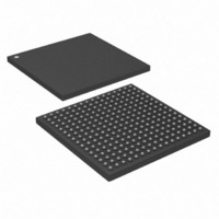
DS26518GN+ Maxim Integrated Products, DS26518GN+ Datasheet - Page 34

DS26518GN+
Manufacturer Part Number
DS26518GN+
Description
IC TXRX T1/E1/J1 8PORT 256-CSBGA
Manufacturer
Maxim Integrated Products
Type
Transceiverr
Specifications of DS26518GN+
Number Of Drivers/receivers
8/8
Protocol
T1/E1/J1
Voltage - Supply
3.135 V ~ 3.465 V
Mounting Type
Surface Mount
Package / Case
256-CSBGA
Lead Free Status / RoHS Status
Lead free / RoHS Compliant
- Current page: 34 of 286
- Download datasheet (2Mb)
9.4
9.4.1 Example Device Initialization and Sequence
STEP 1: Reset the device by pulling the RESETB pin low, applying power to the device, or by using the software
reset bits outlined in Section 9.2.2. Clear all reset bits. Allow time for the reset recovery.
STEP 2: Check the Device ID in the
STEP 3: Write the
follows this write with at least a 300ns delay in order to allow the clock system to properly adjust.
STEP 4: Write the entire remainder of the register space for each port with 00h, including reserved register
locations.
STEP 5: Choose T1/J1 or E1 operation for the framers by configuring the T1/E1 bit in the
registers for each framer. Set the FRM_EN bit to 1 in the
signaling in E1 mode, program the
Control Registers (TCR1–TCR4). Configure the framer Receive Control Registers (RCR1–RCR3). Configure other
framer features as appropriate.
STEP 6: Choose T1/J1 or E1 operation for the LIUs by configuring the T1J1E1S bit in the
Configure the line build-out for each LIU. Configure other LIU features as appropriate. Set the TE (transmit enable)
bit to turn on the TTIPn and TRINGn outputs.
STEP 7: Configure the elastic stores, HDLC controller, and BERT as needed.
STEP 8: Set the INIT_DONE bit in the
9.5
All eight framers share a common microprocessor port and a common MCLK. There is a common software
configurable BPCLK1 output. A set of global registers includes global resets, global interrupt status, interrupt
masking, clock configuration, and the device ID register. See the global register bit map in
JTAG controller is used for all ports.
9.6
Each port has an associated framer, LIU, BERT, jitter attenuator, and transmit/receive HDLC controller. Each of the
per-port functions has its own register space.
9.7
Figure 9-10
information registers and mask bits to the interrupt pin. When an interrupt occurs, the host can read the global
interrupt information registers GFISR1, GLISR1, and
(are) causing the interrupt(s). The host can then read the specific transceiver’s interrupt information registers (TIIR,
RIIR) and the latched status registers (LLSR, BLSR) to further identify the source of the interrupt(s). If TIIR or RIIR
is the source, the host reads the transmit latched status or the receive latched status registers for the source of the
interrupt. All interrupt information register bits are real-time bits that clear once the appropriate interrupt has been
serviced and cleared, as long as no additional, unmasked interrupt condition is present in the associated status
register. All latched status bits must be cleared by the host writing a “1” to the bit location of the interrupt condition
that has been serviced. Latched status bits that have been masked via the interrupt mask registers are masked
from the interrupt information registers. The interrupt mask register bits prevent individual latched status conditions
from generating an interrupt, but they do not prevent the latched status bits from being set. Therefore, when
servicing interrupts, the user should XOR the latched status with the associated interrupt mask in order to exclude
bits for which the user wished to prevent interrupt service. This architecture allows the application host to
periodically poll the latched status bits for noninterrupt conditions, while using only one set of registers.
Initialization and Configuration
Global Resources
Per-Port Resources
Device Interrupts
diagrams the flow of interrupt conditions from their source status bits through the multiple levels of
GTCCR1
register to correctly configure the system clocks. If supplying a 1.544MHz MCLK
IDR
E1TAF
TMMR
register.
and
and
RMMR
E1TNAF
34 of 286
GBISR1
registers for each framer.
TMMR
registers as required. Configure the framer Transmit
to quickly identify which of the eight transceivers is
and
RMMR
DS26518 8-Port T1/E1/J1 Transceiver
registers. If using software transmit
Table
TMMR
LTRCR
10-6. A common
and
register.
RMMR
Related parts for DS26518GN+
Image
Part Number
Description
Manufacturer
Datasheet
Request
R

Part Number:
Description:
8-port T1/e1/j1 Transceiver
Manufacturer:
Maxim Integrated Products, Inc.
Datasheet:

Part Number:
Description:
Ds26518 8-port T1/e1/j1 Transceiver
Manufacturer:
Maxim Integrated Products, Inc.

Part Number:
Description:
power light source LUXEON� Collimator
Manufacturer:
LUMILEDS [Lumileds Lighting Company]
Datasheet:

Part Number:
Description:
MAX7528KCWPMaxim Integrated Products [CMOS Dual 8-Bit Buffered Multiplying DACs]
Manufacturer:
Maxim Integrated Products
Datasheet:

Part Number:
Description:
Single +5V, fully integrated, 1.25Gbps laser diode driver.
Manufacturer:
Maxim Integrated Products
Datasheet:

Part Number:
Description:
Single +5V, fully integrated, 155Mbps laser diode driver.
Manufacturer:
Maxim Integrated Products
Datasheet:

Part Number:
Description:
VRD11/VRD10, K8 Rev F 2/3/4-Phase PWM Controllers with Integrated Dual MOSFET Drivers
Manufacturer:
Maxim Integrated Products
Datasheet:

Part Number:
Description:
Highly Integrated Level 2 SMBus Battery Chargers
Manufacturer:
Maxim Integrated Products
Datasheet:

Part Number:
Description:
Current Monitor and Accumulator with Integrated Sense Resistor; ; Temperature Range: -40°C to +85°C
Manufacturer:
Maxim Integrated Products

Part Number:
Description:
TSSOP 14/A�/RS-485 Transceivers with Integrated 100O/120O Termination Resis
Manufacturer:
Maxim Integrated Products

Part Number:
Description:
TSSOP 14/A�/RS-485 Transceivers with Integrated 100O/120O Termination Resis
Manufacturer:
Maxim Integrated Products

Part Number:
Description:
QFN 16/A�/AC-DC and DC-DC Peak-Current-Mode Converters with Integrated Step
Manufacturer:
Maxim Integrated Products

Part Number:
Description:
TDFN/A/65V, 1A, 600KHZ, SYNCHRONOUS STEP-DOWN REGULATOR WITH INTEGRATED SWI
Manufacturer:
Maxim Integrated Products

Part Number:
Description:
Integrated Temperature Controller f
Manufacturer:
Maxim Integrated Products


