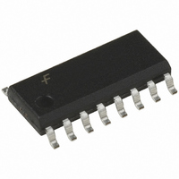
FIN1032MX Fairchild Semiconductor, FIN1032MX Datasheet - Page 3

FIN1032MX
Manufacturer Part Number
FIN1032MX
Description
IC RCVR QUAD 3.3V HS LVDS 16SOIC
Manufacturer
Fairchild Semiconductor
Type
Receiverr
Datasheet
1.FIN1032MX.pdf
(6 pages)
Specifications of FIN1032MX
Number Of Drivers/receivers
0/4
Protocol
LVDS
Voltage - Supply
3 V ~ 3.6 V
Mounting Type
Surface Mount
Package / Case
16-SOIC (3.9mm Width)
Rohs Compliant
YES
Logic Family
FIN10
Logic Type
High Speed Differential Receiver
Supply Voltage (max)
3.6 V
Supply Voltage (min)
3 V
Maximum Operating Temperature
+ 85 C
Mounting Style
SMD/SMT
Data Rate
400 Mbps
Minimum Operating Temperature
- 40 C
Number Of Lines (input / Output)
1 / 1
Propagation Delay Time
2.5 ns
Supply Current
15 mA
Lead Free Status / RoHS Status
Lead free / RoHS Compliant
Other names
FIN1032MXTR
FIN1032MX_NL
FIN1032MX_NLTR
FIN1032MX_NLTR
FIN1032MX_NL
FIN1032MX_NLTR
FIN1032MX_NLTR
Available stocks
Company
Part Number
Manufacturer
Quantity
Price
Company:
Part Number:
FIN1032MX
Manufacturer:
FSC
Quantity:
10 171
Part Number:
FIN1032MX
Manufacturer:
FAIRCHILD/仙童
Quantity:
20 000
t
t
t
t
t
t
t
t
f
t
t
t
t
PLH
PHL
TLH
THL
SK(P)
SK(LH)
SK(HL)
SK(PP)
MAX
ZH
ZL
HZ
LZ
AC Electrical Characteristics
Over supply voltage and operating temperature ranges, unless otherwise specified
Note 3: All typical values are at T
Note 4: t
tion.
Note 5: t
(either LOW-to-HIGH or HIGH-to-LOW) when both devices operate with the same supply voltage, same temperature, and have identical test circuits.
Note 6: f
All channels switching in phase.
Note A: All input pulses have frequency
Note B: C
Symbol
FIGURE 1. Differential Receiver Voltage Definitions and Propagation Delay and Transition Time Test Circuit
SK(LH)
SK(PP)
MAX
L
includes all probe and jig capacitances
Propagation Delay LOW-to-HIGH
Propagation Delay HIGH-to-LOW
Output Rise Time (20% to 80%)
Output Fall Time (80% to 20%)
Pulse Skew |t
Channel-to-Channel Skew
(Note 4)
Part-to-Part Skew (Note 5)
Maximum Operating Frequency
(Note 6)
LVTTL Output Enable Time from Z to HIGH
LVTTL Output Enable Time from Z to LOW
LVTTL Output Disable Time from HIGH to Z
LVTTL Output Disable Time from LOW to Z
Criteria: Input t
, t
is the magnitude of the difference in propagation delay times between any specified terminals of two devices switching in the same direction
SK(HL)
is the skew between specified outputs of a single device when the outputs have identical loads and are switching in the same direc-
1.25
1.15
Applied Voltages (V)
V
2.4
2.3
0.1
1.5
0.9
2.4
1.8
0.6
0
0
IA
TABLE 1. Receiver Minimum and Maximum Input Threshold Test Voltages
PLH
R
= t
- t
F
Parameter
A
PHL
1 ns, V
25 C and with V
|
10MHz, t
ID
1.15
1.25
V
2.3
2.4
0.1
0.9
1.5
1.8
2.4
0.6
0
0
300 mV, (1.05V to 1.35V pp), 50% duty cycle; Output duty cycle 40% to 60%, V
IB
R
CC
or t
F
3.3V.
1ns
Resulting Differential Input
|V
R
See Figure 1 and Figure 2
R
see Figure 1 and Figure 2
R
See Figure 3 and Figure 4
L
L
L
ID
|
Voltage (mA)
1k
1k , C
1k , C
400 mV, C
V
Test Conditions
100
100
100
600
600
600
100
100
100
600
600
600
3
ID
L
L
10 pF,
10 pF,
L
10 pF,
Resulting Common Mode Input
Min
200
1.0
1.0
Voltage (V)
2.35
2.35
0.05
0.05
V
1.2
1.2
1.2
1.2
2.1
2.1
0.3
0.3
IC
(Note 3)
Typ
325
0.7
0.7
OL
www.fairchildsemi.com
0.5V, V
Max
2.5
2.5
1.2
1.2
0.4
0.3
1.0
5.0
5.0
5.0
5.0
OH
2.4V.
Units
MHz
ns
ns
ns
ns
ns
ns
ns
ns
ns
ns
ns


