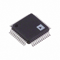
AD9954YSVZ Analog Devices Inc, AD9954YSVZ Datasheet - Page 30

AD9954YSVZ
Manufacturer Part Number
AD9954YSVZ
Description
IC DDS DAC 14BIT 1.8V 48-TQFP
Manufacturer
Analog Devices Inc
Datasheet
1.AD9954YSVZ-REEL7.pdf
(40 pages)
Specifications of AD9954YSVZ
Resolution (bits)
14 b
Master Fclk
400MHz
Tuning Word Width (bits)
32 b
Voltage - Supply
1.71 V ~ 1.96 V
Operating Temperature
-40°C ~ 105°C
Mounting Type
Surface Mount
Package / Case
48-TQFP Exposed Pad, 48-eTQFP, 48-HTQFP, 48-VQFP
Data Rate
25Mbps
Rf Ic Case Style
TQFP
No. Of Pins
48
Supply Voltage Range
1.71V To 1.89V, 3.135V To 3.465V
Operating Temperature Range
-40°C To +105°C
Msl
MSL 3 - 168 Hours
Termination Type
SMD
Rohs Compliant
Yes
Filter Terminals
SMD
Lead Free Status / RoHS Status
Lead free / RoHS Compliant
For Use With
AD9954/PCBZ - BOARD EVAL FOR 9954
Lead Free Status / RoHS Status
Lead free / RoHS Compliant, Lead free / RoHS Compliant
Available stocks
Company
Part Number
Manufacturer
Quantity
Price
Company:
Part Number:
AD9954YSVZ
Manufacturer:
ADI
Quantity:
210
Company:
Part Number:
AD9954YSVZ
Manufacturer:
Analog Devices Inc
Quantity:
10 000
Part Number:
AD9954YSVZ
Manufacturer:
ADI/亚德诺
Quantity:
20 000
Company:
Part Number:
AD9954YSVZ-REEL7
Manufacturer:
UBR
Quantity:
6 000
Company:
Part Number:
AD9954YSVZ-REEL7
Manufacturer:
Analog Devices Inc
Quantity:
10 000
AD9954
CFR1<10>: Clear Phase Accumulator
CFR1<10> = 0 (default). The phase accumulator functions as
normal.
CFR1<10> = 1. The phase accumulator memory elements are
cleared and held clear until this bit is cleared.
CFR1<9>: SDIO Input Only
CFR1<9> = 0 (default). The SDIO pin is bidirectional (2-wire
serial programming mode).
CFR1<9> = 1. The SDIO is configured as an input-only pin
(3-wire serial programming mode).
CFR1<8>: LSB First
CFR1<8> = 0 (default). MSB first format is active.
CFR1<8> = 1. LSB first format is active.
CFR1<7>: Digital Power-Down Bit
CFR1<7> = 0 (default). All digital functions and clocks are active.
CFR1<7> = 1. All non-I/O digital functionality is suspended,
lowering the power significantly.
CFR1<6>: Comparator Power-Down Bit
CFR1<6> = 0 (default). The comparator is enabled for operation.
CFR1<6> = 1. The comparator is disabled and is in its lowest
power dissipation state.
CFR1<5>: DAC Power-Down Bit
CFR1<5> = 0 (default). The DAC is enabled for operation.
CFR1<5> = 1. The DAC is disabled and is in its lowest power
dissipation state.
CFR1<4>: Clock Input Power-Down Bit
CFR1<4> = 0 (default). The clock input circuitry is enabled for
operation.
CFR1<4> = 1. The clock input circuitry is disabled and the
device is in its lowest power dissipation state.
CFR1<3>: External Power-Down Mode
CFR1<3> = 0 (default). The external power-down mode
selected is the rapid recovery power-down mode. In this mode,
when the PWRDWNCTL input pin is high, the digital logic
and the DAC digital logic are powered down. The DAC bias
circuitry, PLL, oscillator, and clock input circuitry are not
powered down. CFR1<6> determines whether the comparator
is powered down. CFR1<7>, and CFR1<5:4> are ignored.
CFR1<3> = 1. The external power-down mode selected is the
full power-down mode. In this mode, when the PWRDWNCTL
input pin is high, all functions are powered down. This includes
the DAC and PLL, which take a significant amount of time to
power up. CFR1<7:4> are all ignored.
Rev. B | Page 30 of 40
CFR1<2>: Linear Sweep No-Dwell Bit
If CFR1<21> is clear, this bit is a don’t care (ignored).
CFR1<2> = 0 (default). The linear sweep no-dwell function is
inactive. If the no-dwell mode is inactive when the sweep
completes, sweeping does not restart until an I/O update or
change in profile initiates another sweep as previously described.
The output frequency holds at the final value in the sweep.
CFR1<2> = 1. The linear sweep no-dwell function is active. If
the no-dwell mode is active when the sweep completes, the
phase accumulator is cleared. The phase accumulator remains
cleared until another sweep is initiated via an I/O update input
or change in profile.
CFR1<1>: SYNC_CLK Disable Bit
CFR1<1> = 0 (default). The SYNC_CLK pin is active.
CFR1<1> = 1. The SYNC_CLK pin assumes a static Logic 0
state to minimize noise generated by the digital circuitry. The
synchronization circuitry remains active internally to maintain
normal device timing.
CFR1<0>: Not Used, Leave Clear
Control Function Register No. 2 (CFR2)
The CFR2 is used to control the various functions, features, and
modes of the AD9954, primarily related to the analog sections
of the chip.
CFR2<23:12>: Not Used, Leave Clear
CFR2<11>: High Speed Sync Enable Bit
CFR2<11> = 0 (default). The high speed sync enhancement is off.
CFR2<11> = 1. The high speed sync enhancement is on. This
bit should be set when using the autosynchronization feature
for SYNC_CLK > 50 MHz (SYSCLK > 200 MSPS).
CFR2<10>: Hardware Manual Sync Enable Bit
CFR2<10> = 0 (default). The hardware manual sync function is off.
CFR2<10> = 1. The hardware manual sync function is enabled.
While this bit is set, a rising edge on the SYNC_IN pin causes
the device to advance the SYNC_CLK rising edge by one
REFCLK cycle. This bit does not self-clear.
CFR2<9>: CRYSTAL OUT Enable Bit
CFR2<9> = 0 (default). The CRYSTAL OUT pin is inactive.
CFR2<9> = 1. The CRYSTAL OUT pin is active. The crystal
oscillator circuitry output drives the CRYSTAL OUT pin, which
can be used as a reference frequency for additional devices.
CFR2<8>: Not Used, Leave Clear
CFR2<7:3>: Reference Clock Multiplier Control Bits
This 5-bit word controls the multiplier value out of the clock-
multiplier (PLL) block. See the Clock Multiplier section for
more details.


