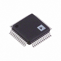
AD9954YSVZ Analog Devices Inc, AD9954YSVZ Datasheet - Page 24

AD9954YSVZ
Manufacturer Part Number
AD9954YSVZ
Description
IC DDS DAC 14BIT 1.8V 48-TQFP
Manufacturer
Analog Devices Inc
Datasheet
1.AD9954YSVZ-REEL7.pdf
(40 pages)
Specifications of AD9954YSVZ
Resolution (bits)
14 b
Master Fclk
400MHz
Tuning Word Width (bits)
32 b
Voltage - Supply
1.71 V ~ 1.96 V
Operating Temperature
-40°C ~ 105°C
Mounting Type
Surface Mount
Package / Case
48-TQFP Exposed Pad, 48-eTQFP, 48-HTQFP, 48-VQFP
Data Rate
25Mbps
Rf Ic Case Style
TQFP
No. Of Pins
48
Supply Voltage Range
1.71V To 1.89V, 3.135V To 3.465V
Operating Temperature Range
-40°C To +105°C
Msl
MSL 3 - 168 Hours
Termination Type
SMD
Rohs Compliant
Yes
Filter Terminals
SMD
Lead Free Status / RoHS Status
Lead free / RoHS Compliant
For Use With
AD9954/PCBZ - BOARD EVAL FOR 9954
Lead Free Status / RoHS Status
Lead free / RoHS Compliant, Lead free / RoHS Compliant
Available stocks
Company
Part Number
Manufacturer
Quantity
Price
Company:
Part Number:
AD9954YSVZ
Manufacturer:
ADI
Quantity:
210
Company:
Part Number:
AD9954YSVZ
Manufacturer:
Analog Devices Inc
Quantity:
10 000
Part Number:
AD9954YSVZ
Manufacturer:
ADI/亚德诺
Quantity:
20 000
Company:
Part Number:
AD9954YSVZ-REEL7
Manufacturer:
UBR
Quantity:
6 000
Company:
Part Number:
AD9954YSVZ-REEL7
Manufacturer:
Analog Devices Inc
Quantity:
10 000
AD9954
SERIAL INTERFACE PORT PIN DESCRIPTIONS
SCLK—Serial Clock. The serial clock pin is used to synchronize
data to and from the AD9954 and to run internal state machines.
SCLK maximum frequency is 25 MHz.
CS —Chip Select. CS is an active low input that enables
devices sharing a serial communications line to be individually
programmed. The SDO and SDIO pins go to a high impedance
state when this input is high. If driven high during any
communications cycle, that cycle is suspended until CS is
reactivated low. Chip select can be tied low if it is not needed.
SDIO —Serial Data I/O. Data written to the AD9954 must be
sent to this pin. However, this pin can be used as a bidirectional
data line. CFR1<9> controls the configuration of this pin.
SDO—Serial Data Out. Data is read from this pin for protocols
that use separate lines for transmitting and receiving data.
When in 2-wire serial programming mode, this pin is set to a
high impedance state.
IOSYNC—synchronizes the I/O port state machines without
affecting the addressable registers contents. An active high input
on the IOSYNC pin aborts the current communication cycle. After
IOSYNC returns low (Logic 0), another communication cycle may
begin, starting with the instruction byte write.
MSB/LSB TRANSFERS
The AD9954 serial port can support either MSB first or LSB
first data formats. This functionality is controlled by the LSB
First Bit CFR1<8>.
For MSB first operation, the serial port controller generates the
most significant byte (of the specified register) address first
followed by the next lesser significant byte addresses until the
I/O operation is complete. All data written to (read from) the
AD9954 must be in MSB first order.
If the LSB mode is active, the serial port controller generates the
least significant byte address first followed by the next greater
significant byte addresses until the I/O operation is complete.
All data written to (read from) the AD9954 must be in LSB
first order.
Example Operation
As an example, consider the case of writing the amplitude scale
factor (ASF) register to a value of 0.5 full scale. First, calculate
the binary equivalent of 0.5. As the ASF is 16 bits wide, the
hexadecimal equivalent is 0x80. Next, for MSB first format,
transmit an instruction byte of 0x02 (serial address of ASF is
00010(b)). From this instruction, the internal controller polls
SCLK
SDIO
CS
I
7
I
6
Figure 28. 2-Wire Serial Port Read Timing—Clock Stall High
INSTRUCTION CYCLE
I
5
I
4
I
3
I
2
Rev. B | Page 24 of 40
I
1
I
0
the register at this memory location and notes that the ASF is
2 bytes wide. The serial port controller’s state machines sets to
16 and awaits 16 rising edges on the SCLK and 16 bits of data
on the SDIO line. Send 16 rising edges on SCLK, and the binary
data 10000000 00000000 on the SDIO line.
To write the amplitude scale factor register in LSB first format,
the process is the same as in MSB first; however, the data is bit
wise inverted on a word-by-word basis. The instruction byte is
0x40. The binary data for the ASF is 00000000 00000001.
SCLK
RAM I/O VIA SERIAL PORT
Accessing the RAM via the serial port is identical to any other
serial I/O operation except that the number of bytes transferred
is determined by the address space between the beginning
address and the final address as specified in the current RAM
segment control word (RSCW). The final address describes the
most significant word address for all I/O transfers and the
beginning address specifies the least significant address.
RAM I/O supports MSB/LSB first operation as set using the
LSB First Bit CFR1<8>. When in MSB first mode, the first data
byte is for the most significant byte of the memory address
described by the final address with the remaining three bytes
making up the lesser significant bytes of that address. The
remaining bytes come in most significant to least significant,
destined for RAM addresses generated in descending order
SDIO
D
CS
O 7
D
O 6
SCLK
DATA TRANSFER CYCLE
SDIO
SDO
TCSU
Figure 29. Timing Diagram for Data Write to AD9954
Figure 30. Timing Diagram for Data Read to AD9954
D
O 5
D
O 4
DVDD I/O = 3.3V
D
TCSU = 3ns
TDSU = 3ns
TDH = 0ns
O 3
D
TDSU
O 2
D
O 1
D
TDV = 25ns
DVDD I/O = 1.8V
TDH
O 0
TCSU = 5ns
TDSU = 5ns
TDH = 0ns
● ● ●
● ● ●
● ● ●
TDH


