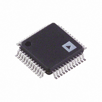
AD9954YSVZ Analog Devices Inc, AD9954YSVZ Datasheet - Page 20

AD9954YSVZ
Manufacturer Part Number
AD9954YSVZ
Description
IC DDS DAC 14BIT 1.8V 48-TQFP
Manufacturer
Analog Devices Inc
Datasheet
1.AD9954YSVZ-REEL7.pdf
(40 pages)
Specifications of AD9954YSVZ
Resolution (bits)
14 b
Master Fclk
400MHz
Tuning Word Width (bits)
32 b
Voltage - Supply
1.71 V ~ 1.96 V
Operating Temperature
-40°C ~ 105°C
Mounting Type
Surface Mount
Package / Case
48-TQFP Exposed Pad, 48-eTQFP, 48-HTQFP, 48-VQFP
Data Rate
25Mbps
Rf Ic Case Style
TQFP
No. Of Pins
48
Supply Voltage Range
1.71V To 1.89V, 3.135V To 3.465V
Operating Temperature Range
-40°C To +105°C
Msl
MSL 3 - 168 Hours
Termination Type
SMD
Rohs Compliant
Yes
Filter Terminals
SMD
Lead Free Status / RoHS Status
Lead free / RoHS Compliant
For Use With
AD9954/PCBZ - BOARD EVAL FOR 9954
Lead Free Status / RoHS Status
Lead free / RoHS Compliant, Lead free / RoHS Compliant
Available stocks
Company
Part Number
Manufacturer
Quantity
Price
Company:
Part Number:
AD9954YSVZ
Manufacturer:
ADI
Quantity:
210
Company:
Part Number:
AD9954YSVZ
Manufacturer:
Analog Devices Inc
Quantity:
10 000
Part Number:
AD9954YSVZ
Manufacturer:
ADI/亚德诺
Quantity:
20 000
Company:
Part Number:
AD9954YSVZ-REEL7
Manufacturer:
UBR
Quantity:
6 000
Company:
Part Number:
AD9954YSVZ-REEL7
Manufacturer:
Analog Devices Inc
Quantity:
10 000
AD9954
The last method in which the sweep ramp rate timer can be
reset is changing from inactive linear sweep mode to active
linear sweep mode using the linear sweep enable bit (CFR1<21>).
For methods two and three, the ramp rate timer loads a value
determined by the state of PS0 (0 = FSRRW, 1 = RSRRW).
Power-Down Functions of the AD9954
The AD9954 supports an externally controlled (or hardware)
power-down feature as well as software-programmable power-
down bits capable of individually powering down specific unused
circuit blocks.
Table 9. Power-Down Control Functions
Control
PWRDWNCTL = 0, CFR1<3> don’t care
PWRDWNCTL = 1, CFR1<3> = 0
PWRDWNCTL = 1, CFR1<3> = 1
Mode Active
Software control
External control, fast recovery
power-down mode
External control, full power-down
mode
Rev. B | Page 20 of 40
Software-controlled power-down enables individual powering
down of the DAC, comparator, PLL, input clock circuitry, and
the digital logic (CFR1<7:4>). With the exception of CFR1<6>,
these bits are superseded when the externally controlled power-
down pin (PWRDWNCTL) is high. External power-down
control is supported on the AD9954 via the PWRDWNCTL
input pin. When the PWRDWNCTL input pin is high, the
AD9954 enters a power-down mode based on the CFR1<3> bit.
When the PWRDWNCTL input pin is low, it operates normally.
See CFR1<3> in Table 12 for details.
Table 9 details the logic level for each power-down bit that
drives out of the AD9954 core logic to the analog section and
the digital clock generation section of the chip for the external
power-down operation.
Description
Digital power-down = CFR1<7>
Comparator power-down = CFR1<6>
DAC power-down = CFR1<5>
Clock input power-down = CFR1<4>
Digital power-down = 1’b1
Comparator power-down = 1’b0 or CFR1<6>
DAC power-down = 1’b0
Clock input power-down = 1’b0
Digital power-down = 1’b1
Comparator power-down = 1’b1
DAC power-down = 1’b1
Clock input power-down = 1’b1


