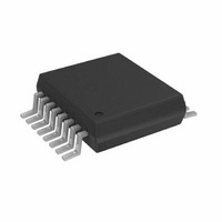
AD5933YRSZ Analog Devices Inc, AD5933YRSZ Datasheet - Page 26

AD5933YRSZ
Manufacturer Part Number
AD5933YRSZ
Description
IC NTWK ANALYZER 12B 1MSP 16SSOP
Manufacturer
Analog Devices Inc
Datasheet
1.AD5933YRSZ.pdf
(44 pages)
Specifications of AD5933YRSZ
Resolution (bits)
12 b
Master Fclk
16.776MHz
Voltage - Supply
2.7 V ~ 5.5 V
Operating Temperature
-40°C ~ 125°C
Mounting Type
Surface Mount
Package / Case
16-SSOP
Supply Voltage Range
2.7V To 5.5V
Operating Temperature Range
-40°C To +125°C
Digital Ic Case Style
SSOP
No. Of Pins
16
Frequency Max
0.1MHz
Termination Type
SMD
Pin Count
16
Screening Level
Automotive
Package Type
SSOP
Filter Terminals
SMD
Rohs Compliant
Yes
Communication Function
Network Analyzer
Lead Free Status / RoHS Status
Lead free / RoHS Compliant
For Use With
EVAL-AD5933EBZ - BOARD EVALUATION FOR AD5933
Tuning Word Width (bits)
-
Lead Free Status / Rohs Status
Compliant
Other names
AD5933BRSZ
Q2204656A
Q2204656A
Available stocks
Company
Part Number
Manufacturer
Quantity
Price
Company:
Part Number:
AD5933YRSZ
Manufacturer:
ADI
Quantity:
5 000
Company:
Part Number:
AD5933YRSZ
Manufacturer:
Fujitsu
Quantity:
500
Part Number:
AD5933YRSZ
Manufacturer:
ADI/亚德诺
Quantity:
20 000
AD5933
FREQUENCY INCREMENT REGISTER (REGISTER
ADDRESS 0x85, REGISTER ADDRESS 0x86,
REGISTER ADDRESS 0x87)
The default value upon reset is as follows: D23 to D0 are not reset
on power-up. After a reset command, the contents of this register
are not reset.
The frequency increment register contains a 24-bit represen-
tation of the frequency increment between consecutive frequency
points along the sweep. For example, if the user requires an
increment step of 10 Hz using a 16.0 MHz clock, the user
should program the value of 0x00 to Register Address 0x85, the
value of 0x01 to Register Address 0x86m, and the value of 0x4F
to Register Address 0x87.
The formula for calculating the increment frequency is given by
The user programs the value 0x00 to Register Address 0x85, the
value 0x01 to Register Address 0x86, and the value 0x4F to
Register Address 0x87.
NUMBER OF INCREMENTS REGISTER (REGISTER
ADDRESS 0x88, REGISTER ADDRESS 0x89)
The default value upon reset is as follows: D8 to D0 are not reset
on power-up. After a reset command, the contents of this
register are not reset.
Table 12. Number of Increments Register
Reg
0x88
0x89
Table 13. Number of Settling Times Cycles Register
Register
0x8A
0x8B
Frequency
Bits
D15 to D9
D8
D8 to D0
Increment
Bits
D15 to D11
D10 to D9
D8
D7 to D0
Description
Don’t care
Number of
increments
Number of
increments
Code
=
⎛
⎜
⎜
⎜
⎜
⎜
⎝
⎛
⎜
⎝
16
Read or
Description
Don’t care
2-bit decode
D10
0
0
1
1
MSB number of settling time cycles
Number of settling time cycles
10
Function
write
Read or
write
Read or
write
MHz
4
Hz
⎞
⎟
⎠
⎞
⎟
⎟
⎟
⎟
⎟
⎠
×
D9
0
1
0
1
2
Format
Integer number
stored in binary
format
Integer number
stored in binary
format
27
≡
x 0
00014
Description
Default
No. of cycles × 2
Reserved
No. of cycles × 4
Rev. C | Page 26 of 44
F
This register determines the number of frequency points in the
frequency sweep. The number of points is represented by a 9-bit
word, D8 to D0. D15 to D9 are don’t care bits. This register, in
conjunction with the start frequency register and the increment
frequency register, determines the frequency sweep range for
the sweep operation. The maximum number of increments that
can be programmed is 511.
NUMBER OF SETTLING TIME CYCLES
REGISTER (REGISTER ADDRESS 0x8A,
REGISTER ADDRESS 0x8B)
The default value upon reset is as follows: D10 to D0 are not
reset on power-up. After a reset command, the contents of this
register are not reset (see Table 13).
This register determines the number of output excitation cycles
that are allowed to pass through the unknown impedance, after
receipt of a start frequency sweep, increment frequency, or
repeat frequency command, before the ADC is triggered to
perform a conversion of the response signal. The number of
settling time cycles register value determines the delay between
a start frequency sweep/increment frequency /repeat frequency
command and the time an ADC conversion commences. The
number of cycles is represented by a 9-bit word, D8 to D0. The
value programmed into the number of settling time cycles
register can be increased by a factor of 2 or 4 depending upon
the status of bits D10 to D9. The five most significant bits, D15
to D11, are don’t care bits. The maximum number of output
cycles that can be programmed is 511 × 4 = 2044 cycles. For
example, consider an excitation signal of 30 kHz. The
maximum delay between the programming of this frequency
and the time that this signal is first sampled by the ADC is ≈
511 × 4 × 33.33 μs = 68.126 ms. The ADC takes 1024 samples,
and the result is stored as real data and imaginary data in
Register Address 0x94 to Register Address 0x97. The conversion
process takes approximately 1 ms using a 16.777 MHz clock.
Function
Read or write
Read or write
Format
Integer number stored in
binary format


