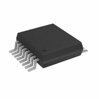
AD5933YRSZ Analog Devices Inc, AD5933YRSZ Datasheet - Page 14

AD5933YRSZ
Manufacturer Part Number
AD5933YRSZ
Description
IC NTWK ANALYZER 12B 1MSP 16SSOP
Manufacturer
Analog Devices Inc
Datasheet
1.AD5933YRSZ.pdf
(44 pages)
Specifications of AD5933YRSZ
Resolution (bits)
12 b
Master Fclk
16.776MHz
Voltage - Supply
2.7 V ~ 5.5 V
Operating Temperature
-40°C ~ 125°C
Mounting Type
Surface Mount
Package / Case
16-SSOP
Supply Voltage Range
2.7V To 5.5V
Operating Temperature Range
-40°C To +125°C
Digital Ic Case Style
SSOP
No. Of Pins
16
Frequency Max
0.1MHz
Termination Type
SMD
Pin Count
16
Screening Level
Automotive
Package Type
SSOP
Filter Terminals
SMD
Rohs Compliant
Yes
Communication Function
Network Analyzer
Lead Free Status / RoHS Status
Lead free / RoHS Compliant
For Use With
EVAL-AD5933EBZ - BOARD EVALUATION FOR AD5933
Tuning Word Width (bits)
-
Lead Free Status / Rohs Status
Compliant
Other names
AD5933BRSZ
Q2204656A
Q2204656A
Available stocks
Company
Part Number
Manufacturer
Quantity
Price
Company:
Part Number:
AD5933YRSZ
Manufacturer:
ADI
Quantity:
5 000
Company:
Part Number:
AD5933YRSZ
Manufacturer:
Fujitsu
Quantity:
500
Part Number:
AD5933YRSZ
Manufacturer:
ADI/亚德诺
Quantity:
20 000
AD5933
TRANSMIT STAGE
As shown in Figure 19, the transmit stage of the AD5933 is made
up of a 27-bit phase accumulator DDS core that provides the
output excitation signal at a particular frequency. The input to
the phase accumulator is taken from the contents of the start
frequency register (see Register Address 0x82, Register Address
0x83, and Register Address 0x84). Although the phase accumu-
lator offers 27 bits of resolution, the start frequency register has
the three most significant bits (MSBs) set to 0 internally; therefore,
the user has the ability to program only the lower 24 bits of the
start frequency register.
The AD5933 offers a frequency resolution programmable by the
user down to 0.1 Hz. The frequency resolution is programmed
via a 24-bit word loaded serially over the I
frequency increment register.
The frequency sweep is fully described by the programming of
three parameters: the start frequency, the frequency increment,
and the number of increments.
Start Frequency
This is a 24-bit word that is programmed to the on-board RAM
at Register Address 0x82, Register Address 0x83, and Register
Address 0x84 (see the Register Map section). The required code
loaded to the start frequency register is the result of the formula
shown in Equation 1, based on the master clock frequency and the
required start frequency output from the DDS.
For example, if the user requires the sweep to begin at 30 kHz and
has a 16 MHz clock signal connected to MCLK, the code that
needs to be programmed is given by
The user programs the value of 0x0F to Register Address 0x82, the
value of 0x5C to Register Address 0x83, and the value of 0x28 to
Register Address 0x84.
⎛
⎜
⎜
⎜
⎜
⎝
Start
Start
Required
ACCUMULATOR
(27 BITS)
Frequency
Frequency
PHASE
Output
⎛
⎜
⎝
MCLK
Code
Code
Figure 19. Transmit Stage
4
Start
=
=
⎞
⎟
⎠
DAC
⎛
⎜
⎜
⎜
⎜
⎜
⎝
Frequency
⎛
⎜
⎝
16
30
V
MHz
BIAS
kHz
4
R(GAIN)
⎞
⎟
⎟
⎟
⎟
⎠
⎞
⎟
⎠
×
⎞
⎟
⎟
⎟
⎟
⎟
⎠
2
C interface to the
×
2
27
2
27
≡
0x0F5C28
VOUT
Rev. C | Page 14 of 44
(1)
Frequency Increment
This is a 24-bit word that is programmed to the on-board RAM
at Register Address 0x85, Register Address 0x86, and Register
Address 0x87 (see the Register Map). The required code loaded
to the frequency increment register is the result of the formula
shown in Equation 2, based on the master clock frequency and the
required increment frequency output from the DDS.
For example, if the user requires the sweep to have a resolution
of 10 Hz and has a 16 MHz clock signal connected to MCLK, the
code that needs to be programmed is given by
The user programs the value of 0x00 to Register Address 0x85,
the value of 0x01 to Register Address 0x86, and the value of 0x4F
to Register Address 0x87.
Number of Increments
This is a 9-bit word that represents the number of frequency
points in the sweep. The number is programmed to the on-board
RAM at Register Address 0x88 and Register Address 0x89 (see the
Register Map section). The maximum number of points that can
be programmed is 511.
For example, if the sweep needs 150 points, the user programs
the value of 0x00 to Register Address 0x88 and the value of 0x96
to Register Address 0x89.
Once the three parameter values have been programmed, the
sweep is initiated by issuing a start frequency sweep command to
the control register at Register Address 0x80 and Register Address
0x81 (see the Register Map section). Bit D2 in the status register
(Register Address 0x8F) indicates the completion of the frequency
measurement for each sweep point. Incrementing to the next
frequency sweep point is under the control of the user. The
measured result is stored in the two register groups that follow:
0x94, 0x95 (real data) and 0x96, 0x97 (imaginary data) that should
be read before issuing an increment frequency command to the
control register to move to the next sweep point. There is the
facility to repeat the current frequency point measurement by
issuing a repeat frequency command to the control register. This
has the benefit of allowing the user to average successive readings.
When the frequency sweep has completed all frequency points,
Bit D3 in the status register is set, indicating completion of the
sweep . Once this bit is set, further increments are disabled.
Frequency
⎛
⎜
⎜
⎜
⎜
⎝
Frequency
Re
quired
Increment
Increment
Frequency
⎛
⎜
⎝
MCLK
4
⎞
⎟
⎠
Code
Code
Increment
=
=
⎛
⎜
⎜
⎜
⎜
⎜
⎝
⎛
⎜
⎝
16
10
⎞
⎟
⎟
⎟
⎟
⎠
×
MHz
4
Hz
2
27
⎞
⎟
⎠
⎞
⎟
⎟
⎟
⎟
⎟
⎠
≡
0x00014F
(2)


