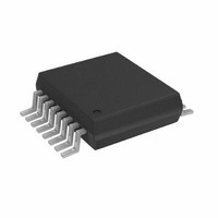
AD5933YRSZ Analog Devices Inc, AD5933YRSZ Datasheet - Page 18

AD5933YRSZ
Manufacturer Part Number
AD5933YRSZ
Description
IC NTWK ANALYZER 12B 1MSP 16SSOP
Manufacturer
Analog Devices Inc
Datasheet
1.AD5933YRSZ.pdf
(44 pages)
Specifications of AD5933YRSZ
Resolution (bits)
12 b
Master Fclk
16.776MHz
Voltage - Supply
2.7 V ~ 5.5 V
Operating Temperature
-40°C ~ 125°C
Mounting Type
Surface Mount
Package / Case
16-SSOP
Supply Voltage Range
2.7V To 5.5V
Operating Temperature Range
-40°C To +125°C
Digital Ic Case Style
SSOP
No. Of Pins
16
Frequency Max
0.1MHz
Termination Type
SMD
Pin Count
16
Screening Level
Automotive
Package Type
SSOP
Filter Terminals
SMD
Rohs Compliant
Yes
Communication Function
Network Analyzer
Lead Free Status / RoHS Status
Lead free / RoHS Compliant
For Use With
EVAL-AD5933EBZ - BOARD EVALUATION FOR AD5933
Tuning Word Width (bits)
-
Lead Free Status / Rohs Status
Compliant
Other names
AD5933BRSZ
Q2204656A
Q2204656A
Available stocks
Company
Part Number
Manufacturer
Quantity
Price
Company:
Part Number:
AD5933YRSZ
Manufacturer:
ADI
Quantity:
5 000
Company:
Part Number:
AD5933YRSZ
Manufacturer:
Fujitsu
Quantity:
500
Part Number:
AD5933YRSZ
Manufacturer:
ADI/亚德诺
Quantity:
20 000
AD5933
TWO-POINT CALIBRATION
Alternatively, it is possible to minimize this error by assuming that
the frequency variation is linear and adjusting the gain factor with
a two-point calibration. Figure 23 shows an impedance profile
based on a two-point gain factor calculation.
TWO-POINT GAIN FACTOR CALCULATION
This is an example of a two-point gain factor calculation assuming
the following:
Typical values of the gain factor calculated at the two calibration
frequencies read
Therefore, the gain factor required at 60 kHz is given by
The required gain factor is 1.033453E-9.
The impedance is calculated as previously described.
Figure 23. Impedance Profile Using a Two-Point Gain Factor Calculation
Output excitation voltage = 2 V (p-p)
Calibration impedance value, Z
PGA gain = ×1
Supply voltage = 3.3 V
Current-to-voltage amplifier gain resistor = 100 kΩ
Calibration frequencies = 55 kHz and 65 kHz
Gain factor calculated at 55 kHz is 1.031224E-09
Gain factor calculated at 65 kHz is 1.035682E-09
Difference in gain factor (ΔGF) is 1.035682E-09 −
1.031224E-09 = 4.458000E-12
Frequency span of sweep (ΔF) = 10 kHz
⎛
⎜
⎜
⎝
. 4
101.5
101.0
100.5
100.0
99.5
99.0
98.5
458000
10
54
VDD = 3.3V
CALIBRATION FREQUENCY = 60kHz
T
MEASURED CALIBRATION IMPEDANCE = 100kΩ
kHz
A
= 25°C
- E
12
56
×
5
kHz
58
FREQUENCY (kHz)
⎞
⎟
⎟
⎠
+
. 1
60
031224
UNKNOWN
62
×
10
= 100.0 kΩ
9 -
64
66
Rev. C | Page 18 of 44
GAIN FACTOR SETUP CONFIGURATION
When calculating the gain factor, it is important that the receive
stage operate in its linear region. This requires careful selection of
the excitation signal range, current-to-voltage gain resistor, and
PGA gain.
The gain through the system shown in Figure 24 is given by
For this example, assume the following system settings:
The peak-to-peak voltage presented to the ADC input is
2 V p-p. However, if a PGA gain of ×5 was chose, the voltage
would saturate the ADC.
GAIN FACTOR RECALCULATION
The gain factor must be recalculated for a change in any of the
following parameters:
•
•
•
VOUT
VDD = 3.3 V
Gain setting resistor = 200 kΩ
Z
PGA setting = ×1
Current-to-voltage gain setting resistor
Output excitation voltage
PGA gain
Ouput
Gain
UNKNOWN
Z
Setting
Z
UNKNOWN
Excitation
UNKNOWN
= 200 kΩ
VDD/2
GAIN SETTING RESISTOR
CURRENT-TO-VOLTAGE
Re
VIN
Figure 24. System Voltage Gain
sistor
Voltage
×
PGA
RFB
Range
Gain
(×1 OR ×5)
×
PGA
LPF
ADC


