DS31412 Maxim Integrated Products, DS31412 Datasheet - Page 24
DS31412
Manufacturer Part Number
DS31412
Description
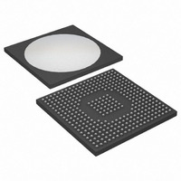
IC 12CH DS3/3 FRAMER 349-BGA
Manufacturer
Maxim Integrated Products
Datasheet
1.DS3148.pdf
(89 pages)
Specifications of DS31412
Controller Type
DS3/E3 Framer
Interface
LIU
Voltage - Supply
3.135 V ~ 3.465 V
Current - Supply
960mA
Operating Temperature
-40°C ~ 85°C
Mounting Type
Surface Mount
Package / Case
349-BGA
Lead Free Status / RoHS Status
Lead free / RoHS Compliant
Available stocks
Company
Part Number
Manufacturer
Quantity
Price


Register Name:
Register Description:
Register Address:
Bit #
Name
Default
Bit 0: Payload Loopback Enable (PLB). When payload loopback is enabled, the transmit formatter operates from
the receive clock (rather than TICLK) and sources DS3/E3 payload bits from the receive data stream rather than
from the TDAT input pin. Receive data is still available on the RDAT output pin during payload loopback. See
Figure 1-1
Bit 1: Line Loopback Enable (LLB). Line loopback connects the TPOS, TNEG, and TCLK output pins to the
RPOS, RNEG, and RCLK input pins. When line loopback is enabled, the receive framer continues to process the
incoming receive data stream and present it on the RDAT pin; the output of the transmit formatter is ignored. Line
loopback and diagnostic loopback can be active at the same time to support simultaneous local and far-end
loopbacks. See
Bit 2: Diagnostic Loopback Enable (DLB). When diagnostic loopback is enabled, the receive framer sources
data from the transmit formatter rather than the RCLK, RPOS, and RNEG input pins. Transmit data is sourced prior
to transmit AIS generation, unframed all ones generation, TCLK/TPOS/TNEG pin inversion, and TPOS/TNEG
force-high logic. This allows the device to transmit AIS or unframed all ones to the far end while locally looping
back the actual transmit data stream, which could be test patterns or other traffic that should not be sent to the far
end. See
Bit 4: Receive Zero Suppression Code Format (RZSF). When RZSF is set to logic 0, the B3ZS/HDB3 decoder
declares a B3ZS codeword when it sees a zero followed by a BPV that has the opposite polarity as the previous
BPV, and an HDB3 codeword when it sees two zeros followed by a BPV that has the opposite polarity as the
previous BPV. When RZSF is set to logic 1, the polarity of the previous BPV is not considered, and the decoder
declares a B3ZS codeword when it sees a zero followed by a BPV and an HDB3 codeword when it sees two zeros
followed by a BPV.
Bit 6: Transmit Constant Clock Select (TCCLK). When TCCLK is set to logic 1, the device outputs a constant
transmit clock on the TDEN/TGCLK pin instead of a data enable or gapped clock. This bit has precedence over the
TDENMS bit in register MC3. The pin can still be inverted by MC3:TDENI.
Bit 7: One-Second Timer Clock Select (OSTCS). This control bit selects the clock source for the internal one-
second timer.
0 = disable payload loopback
1 = enable payload loopback
0 = disable line loopback
1 = enable line loopback
0 = disable diagnostic loopback
1 = enable diagnostic loopback
0 = the function of the TDEN/TGCLK pin is controlled by TDENMS control bit
1 = the TDEN/TGCLK pin is a constant transmit clock output
0 = use RCLK
1 = use TICLK
Figure 1-1
for a visual description of this loopback.
OSTCS
Figure 1-1
7
0
for a visual description of this loopback.
TCCLK
for a visual description of this loopback.
6
0
MC2
Master Configuration Register 2
02h
N/A
—
5
RZSF
24 of 89
—
4
N/A
—
3
DLB
2
0
LLB
1
0
PLB
0
0
Related parts for DS31412
Image
Part Number
Description
Manufacturer
Datasheet
Request
R

Part Number:
Description:
MAX7528KCWPMaxim Integrated Products [CMOS Dual 8-Bit Buffered Multiplying DACs]
Manufacturer:
Maxim Integrated Products
Datasheet:
Part Number:
Description:
Single +5V, fully integrated, 1.25Gbps laser diode driver.
Manufacturer:
Maxim Integrated Products
Datasheet:
Part Number:
Description:
Single +5V, fully integrated, 155Mbps laser diode driver.
Manufacturer:
Maxim Integrated Products
Datasheet:
Part Number:
Description:
VRD11/VRD10, K8 Rev F 2/3/4-Phase PWM Controllers with Integrated Dual MOSFET Drivers
Manufacturer:
Maxim Integrated Products
Datasheet:
Part Number:
Description:
Highly Integrated Level 2 SMBus Battery Chargers
Manufacturer:
Maxim Integrated Products
Datasheet:
Part Number:
Description:
Current Monitor and Accumulator with Integrated Sense Resistor; ; Temperature Range: -40°C to +85°C
Manufacturer:
Maxim Integrated Products
Part Number:
Description:
TSSOP 14/A�/RS-485 Transceivers with Integrated 100O/120O Termination Resis
Manufacturer:
Maxim Integrated Products
Part Number:
Description:
TSSOP 14/A�/RS-485 Transceivers with Integrated 100O/120O Termination Resis
Manufacturer:
Maxim Integrated Products
Part Number:
Description:
QFN 16/A�/AC-DC and DC-DC Peak-Current-Mode Converters with Integrated Step
Manufacturer:
Maxim Integrated Products
Part Number:
Description:
TDFN/A/65V, 1A, 600KHZ, SYNCHRONOUS STEP-DOWN REGULATOR WITH INTEGRATED SWI
Manufacturer:
Maxim Integrated Products
Part Number:
Description:
Integrated Temperature Controller f
Manufacturer:
Maxim Integrated Products
Part Number:
Description:
SOT23-6/I�/45MHz to 650MHz, Integrated IF VCOs with Differential Output
Manufacturer:
Maxim Integrated Products
Part Number:
Description:
SOT23-6/I�/45MHz to 650MHz, Integrated IF VCOs with Differential Output
Manufacturer:
Maxim Integrated Products
Part Number:
Description:
EVALUATION KIT/2.4GHZ TO 2.5GHZ 802.11G/B RF TRANSCEIVER WITH INTEGRATED PA
Manufacturer:
Maxim Integrated Products
Part Number:
Description:
QFN/E/DUAL PCIE/SATA HIGH SPEED SWITCH WITH INTEGRATED BIAS RESISTOR
Manufacturer:
Maxim Integrated Products
Datasheet: