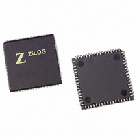
Z16C3510VSG Zilog, Z16C3510VSG Datasheet - Page 65

Z16C3510VSG
Manufacturer Part Number
Z16C3510VSG
Description
IC 10MHZ Z8500 CMOS ISCC 68-PLCC
Manufacturer
Zilog
Series
IUSC™r
Specifications of Z16C3510VSG
Controller Type
Serial Communications Controller (SCC)
Interface
USB
Voltage - Supply
4.75 V ~ 5.25 V
Current - Supply
50mA
Operating Temperature
0°C ~ 70°C
Mounting Type
Surface Mount
Package / Case
68-LCC (J-Lead)
Lead Free Status / RoHS Status
Lead free / RoHS Compliant
Available stocks
Company
Part Number
Manufacturer
Quantity
Price
- Current page: 65 of 268
- Download datasheet (3Mb)
UM011001-0601
Bit combination 110 is the Error Reset Command
This command resets the error bits in RR1. If interrupt on
first Rx Character or interrupt on Special Condition modes
are selected and a special condition exists, the data with
the special condition is held in the receive FIFO until this
command is issued. If either of these modes is selected
and this command is issued before the data has been read
from the receive FIFO, the data is lost.
Bit combination 111 is the Reset Highest IUS
Command
This command resets the highest priority Interrupt Under
Service (IUS) bit, allowing lower priority conditions to re-
quest interrupts. This command allows the use of the inter-
nal daisy-chain (even in systems without an external dai-
sy-chain) and should be the last operation in an interrupt
service routine.
Bits 2 through 0 are the Register Selection Code when the
device is programmed to be in the non-multiplexed bus
mode. These three bits select Registers 0 through 7. With
the Point High command, Registers 8 through 15 are se-
lected.
In the multiplexed bus mode, bits D2 through D0 have the
following function.
Bit D2 must be programmed as “0.” Bits D1 and D0 select
Shift Left/Right; that is WR0(1-0)=10 for shift left and
WR0(1-0)=11 for shift right.
5.4.2 Write Register 1 (Transmit/Receive In-
terrupt and Data Transfer Mode Definition)
Write Register 1 is the control register for the various SCC
cell interrupt and Wait/Request modes. Figure 5-3 shows
the bit assignments for WR1.
P R E L I M I N A R Y
A1/A//B
A1/A//B
Using Pointer (Non-Multiplexed Bus Mode)
Table 5-4. SCC Cell Register Address Map
0
0
0
0
0
0
0
0
1
1
1
1
1
1
1
1
0
0
0
0
0
0
0
0
1
1
1
1
1
1
1
1
Using Point High Command
D2 D1 D0
D2 D1 D0
Using Null Command
Address
Address
000
001
010
011
100
101
110
111
000
001
010
011
100
101
110
111
000
001
010
011
100
101
110
111
000
001
010
011
100
101
110
111
Z16C35ISCC™ User’s Manual
Register
Register
WR10B
WR11B
WR12B
WR13B
WR14B
WR15B
WR10A
WR11A
WR12A
WR13A
WR14A
WR15A
WR0B
WR1B
WR3B
WR4B
WR5B
WR6B
WR7B
WR0A
WR1A
WR3A
WR4A
WR5A
WR6A
WR7A
WR8B
WR8A
WR9A
Write
WR2
WR2
Write
WR9
Register Descriptions
Register
Register
(RR13B)
(RR15B)
(RR10B)
(RR13A)
(RR15A)
(RR10A)
(RR0B)
(RR1B)
(RR2B)
(RR3B)
(RR0A)
(RR1A)
(RR2A)
(RR3A)
RR10B
RR12B
RR13B
RR15B
RR10A
RR12A
RR13A
RR15A
RR0B
RR1B
RR2B
RR3B
RR0A
RR1A
RR2A
RR3A
Read
RR8B
RR8A
Read
5-5
5
Related parts for Z16C3510VSG
Image
Part Number
Description
Manufacturer
Datasheet
Request
R

Part Number:
Description:
CMOS ISCC INTEGRATED SERIAL COMMUNICATIONS CONTROLLER
Manufacturer:
ZILOG [Zilog, Inc.]
Datasheet:

Part Number:
Description:
Communication Controllers, ZILOG INTELLIGENT PERIPHERAL CONTROLLER (ZIP)
Manufacturer:
Zilog, Inc.
Datasheet:

Part Number:
Description:
KIT DEV FOR Z8 ENCORE 16K TO 64K
Manufacturer:
Zilog
Datasheet:

Part Number:
Description:
KIT DEV Z8 ENCORE XP 28-PIN
Manufacturer:
Zilog
Datasheet:

Part Number:
Description:
DEV KIT FOR Z8 ENCORE 8K/4K
Manufacturer:
Zilog
Datasheet:

Part Number:
Description:
KIT DEV Z8 ENCORE XP 28-PIN
Manufacturer:
Zilog
Datasheet:

Part Number:
Description:
DEV KIT FOR Z8 ENCORE 4K TO 8K
Manufacturer:
Zilog
Datasheet:

Part Number:
Description:
CMOS Z8 microcontroller. ROM 16 Kbytes, RAM 256 bytes, speed 16 MHz, 32 lines I/O, 3.0V to 5.5V
Manufacturer:
Zilog, Inc.
Datasheet:

Part Number:
Description:
Low-cost microcontroller. 512 bytes ROM, 61 bytes RAM, 8 MHz
Manufacturer:
Zilog, Inc.
Datasheet:

Part Number:
Description:
Z8 4K OTP Microcontroller
Manufacturer:
Zilog, Inc.
Datasheet:

Part Number:
Description:
CMOS SUPER8 ROMLESS MCU
Manufacturer:
Zilog, Inc.
Datasheet:

Part Number:
Description:
SL1866 CMOSZ8 OTP Microcontroller
Manufacturer:
Zilog, Inc.
Datasheet:

Part Number:
Description:
SL1866 CMOSZ8 OTP Microcontroller
Manufacturer:
Zilog, Inc.
Datasheet:

Part Number:
Description:
OTP (KB) = 1, RAM = 125, Speed = 12, I/O = 14, 8-bit Timers = 2, Comm Interfaces Other Features = Por, LV Protect, Voltage = 4.5-5.5V
Manufacturer:
Zilog, Inc.
Datasheet:


