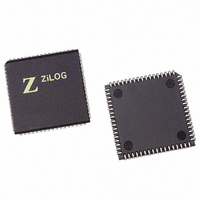
Z16C3510VSG Zilog, Z16C3510VSG Datasheet - Page 28

Z16C3510VSG
Manufacturer Part Number
Z16C3510VSG
Description
IC 10MHZ Z8500 CMOS ISCC 68-PLCC
Manufacturer
Zilog
Series
IUSC™r
Specifications of Z16C3510VSG
Controller Type
Serial Communications Controller (SCC)
Interface
USB
Voltage - Supply
4.75 V ~ 5.25 V
Current - Supply
50mA
Operating Temperature
0°C ~ 70°C
Mounting Type
Surface Mount
Package / Case
68-LCC (J-Lead)
Lead Free Status / RoHS Status
Lead free / RoHS Compliant
Available stocks
Company
Part Number
Manufacturer
Quantity
Price
- Current page: 28 of 268
- Download datasheet (3Mb)
Z16C35ISCC™ User’s Manual
ISCC™ DMA and Ancillary Support Circuitry
3.5 DIGITAL PHASE-LOCKED LOOP (DPLL) (Continued)
3.5.2 DPLL Operation in the FM Modes
To operate in FM mode, the DPLL must be supplied with a
clock that is 16 times the data rate. The DPLL uses this
clock, along with the receive data, to construct receive and
transmit clock outputs that are phased to receive and
transmit data properly.
In FM mode, the transmit clock and receive clock outputs
from the DPLL are not in phase. This is necessary to make
the transmit and receive bit cell boundaries coincide, since
the receive clock must sample the data one-fourth and
three-fourths of the way through the bit cell.
Ordinarily, a bit cell boundary will occur between count 15
or count 16, and the DPLL receive output will cause the
3-8
Correction
Windows
Receive
Length
Output
Count
DPLL
RX DPLL Out
Data
TX DPLL Out
Correction
Bit Cell
+1
Count
32
-1
32
16
No Change
+1
17
+1
-1
18 19 20
32
Figure 3-6. DPLL Operating Example (NRZI Mode)
+1
Figure 3-7. DPLL Operation in the FM Mode
21 22 23 24 25 26 27 28 29 30 31
-1
31
+1
-1
31
+1
31
-1
+1
In FM mode one cycles of the counter in the DPLL is a
count from 0 to 31, but now each cycle corresponds to 2-
bit cells. To make adjustments to remain in phase with the
receive data, the DPLL divides a pair of bit cells into 5
regions, making the adjustment to the counter dependent
upon which region the transition on the receive data input
occurred. This is shown in Figure 3-7.
data to be sampled at one-fourth and three-fourths of the
way through the bit cell.
However, four variations may happen:
1. The DPLL actually allows the transition marking a bit-
33
-1
cell boundary to occur anywhere during the second
half of count 15 or the first half of count 16, without
making a correction to its count cycle.
Ignored
+1
0
33
1
-1
2 3 4 5
+1
33
-1
+1
6
7 8 9
10
UM011001-0601
11
No Change
12 13 14
-1
15
Related parts for Z16C3510VSG
Image
Part Number
Description
Manufacturer
Datasheet
Request
R

Part Number:
Description:
CMOS ISCC INTEGRATED SERIAL COMMUNICATIONS CONTROLLER
Manufacturer:
ZILOG [Zilog, Inc.]
Datasheet:

Part Number:
Description:
Communication Controllers, ZILOG INTELLIGENT PERIPHERAL CONTROLLER (ZIP)
Manufacturer:
Zilog, Inc.
Datasheet:

Part Number:
Description:
KIT DEV FOR Z8 ENCORE 16K TO 64K
Manufacturer:
Zilog
Datasheet:

Part Number:
Description:
KIT DEV Z8 ENCORE XP 28-PIN
Manufacturer:
Zilog
Datasheet:

Part Number:
Description:
DEV KIT FOR Z8 ENCORE 8K/4K
Manufacturer:
Zilog
Datasheet:

Part Number:
Description:
KIT DEV Z8 ENCORE XP 28-PIN
Manufacturer:
Zilog
Datasheet:

Part Number:
Description:
DEV KIT FOR Z8 ENCORE 4K TO 8K
Manufacturer:
Zilog
Datasheet:

Part Number:
Description:
CMOS Z8 microcontroller. ROM 16 Kbytes, RAM 256 bytes, speed 16 MHz, 32 lines I/O, 3.0V to 5.5V
Manufacturer:
Zilog, Inc.
Datasheet:

Part Number:
Description:
Low-cost microcontroller. 512 bytes ROM, 61 bytes RAM, 8 MHz
Manufacturer:
Zilog, Inc.
Datasheet:

Part Number:
Description:
Z8 4K OTP Microcontroller
Manufacturer:
Zilog, Inc.
Datasheet:

Part Number:
Description:
CMOS SUPER8 ROMLESS MCU
Manufacturer:
Zilog, Inc.
Datasheet:

Part Number:
Description:
SL1866 CMOSZ8 OTP Microcontroller
Manufacturer:
Zilog, Inc.
Datasheet:

Part Number:
Description:
SL1866 CMOSZ8 OTP Microcontroller
Manufacturer:
Zilog, Inc.
Datasheet:

Part Number:
Description:
OTP (KB) = 1, RAM = 125, Speed = 12, I/O = 14, 8-bit Timers = 2, Comm Interfaces Other Features = Por, LV Protect, Voltage = 4.5-5.5V
Manufacturer:
Zilog, Inc.
Datasheet:


