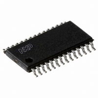
TDA8023TT/C1,118 NXP Semiconductors, TDA8023TT/C1,118 Datasheet - Page 6

TDA8023TT/C1,118
Manufacturer Part Number
TDA8023TT/C1,118
Description
IC SMART CARD INTERFACE 28-TSSOP
Manufacturer
NXP Semiconductors
Datasheet
1.TDA8023TTC1118.pdf
(32 pages)
Specifications of TDA8023TT/C1,118
Package / Case
28-TSSOP
Controller Type
Smart Card Interface
Interface
I²C
Voltage - Supply
2.7 V ~ 6.5 V
Current - Supply
200mA
Operating Temperature
-40°C ~ 85°C
Mounting Type
Surface Mount
Maximum Operating Temperature
+ 85 C
Minimum Operating Temperature
- 40 C
Mounting Style
SMD/SMT
Lead Free Status / RoHS Status
Lead free / RoHS Compliant
Lead Free Status / RoHS Status
Lead free / RoHS Compliant, Lead free / RoHS Compliant
Other names
935274975118
TDA8023TT-T
TDA8023TT-T
TDA8023TT-T
TDA8023TT-T
NXP Semiconductors
8. Functional description
TDA8023_1
Product data sheet
8.2.1 Without external divider on pin PORADJ
8.1 Power supplies
8.2 Voltage supervisor
Remark: Throughout this document, it is assumed that the reader is familiar with
ISO 7816 and EMV 2000 terminology.
The supply pins for the TDA8023 are V
2.7 V to 6.5 V. The supply voltages V
TDA8023 in any time sequence.
All interface signals with the system controller are referenced to a separate supply voltage
V
For generating a supply voltage V
integrated DC-to-DC converter is incorporated. This DC-to-DC converter should be
separately supplied by V
The I
V
The voltage supervisor surveys the V
(POR) and as supply dropout detection during a card session. Supply dropout detection
ensures that a proper deactivation sequence is followed before the voltage is too low. A
reset pulse of duration t
the Inactive mode during powering up or powering down of V
As long as V
on the command lines are. This also lasts for the duration of t
level higher than V
sequence of the contacts is performed.
In this case (no external resistor bridge) it is mandatory to connect pin PORADJ to GND.
Fig 4. Voltage supervisor and Shutdown mode
DD(INTF)
DD
SDWN
.
V
2
INT
DD
C-bus signals SDA and SCL may be externally referenced to a voltage higher than
on pin V
bus unresponsive
DD
power on
is less than V
DDI
th(POR)H
, that may be lower or higher than V
W
Rev. 01 — 16 July 2007
t
DD(DCDC)
W
(see
. When V
status read
th(POR)H
Figure
CC
on pin V
DD
of 5 V
the TDA8023 will remain inactive whatever the levels
DD
DD
4) is used internally for maintaining the TDA8023 in
falls below V
shutdown mode
DD
bus unresponsive
, V
supply voltage. It is used as Power-On Reset
and GND. V
DDP
DD(INTF)
5 % or 3 V
and GNDP (from 2.7 V to 6.5 V).
t
and V
W
th(POR)L
status read
DD
DD(DCDC)
DD
should be in the range from
5 % used by the card, an
.
an automatic deactivation
Low power IC card interface
DD
W
.
after V
may be applied to the
bus unresponsive
power off
DD
TDA8023
© NXP B.V. 2007. All rights reserved.
001aag339
has reached a
V
hys(POR)
V
V
th(POR)H
th(POR)L
6 of 32


