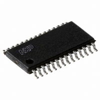
TDA8023TT/C1,118 NXP Semiconductors, TDA8023TT/C1,118 Datasheet - Page 12

TDA8023TT/C1,118
Manufacturer Part Number
TDA8023TT/C1,118
Description
IC SMART CARD INTERFACE 28-TSSOP
Manufacturer
NXP Semiconductors
Datasheet
1.TDA8023TTC1118.pdf
(32 pages)
Specifications of TDA8023TT/C1,118
Package / Case
28-TSSOP
Controller Type
Smart Card Interface
Interface
I²C
Voltage - Supply
2.7 V ~ 6.5 V
Current - Supply
200mA
Operating Temperature
-40°C ~ 85°C
Mounting Type
Surface Mount
Maximum Operating Temperature
+ 85 C
Minimum Operating Temperature
- 40 C
Mounting Style
SMD/SMT
Lead Free Status / RoHS Status
Lead free / RoHS Compliant
Lead Free Status / RoHS Status
Lead free / RoHS Compliant, Lead free / RoHS Compliant
Other names
935274975118
TDA8023TT-T
TDA8023TT-T
TDA8023TT-T
TDA8023TT-T
NXP Semiconductors
TDA8023_1
Product data sheet
8.4.1 Capacitive configuration
8.4 DC-to-DC converter
Table 10.
Table 11.
Table 12.
If bit RSTIN = 0 when bit START is set to logic 1, then pin RST is controlled by bit RSTIN.
Else, pin RST = LOW during a number of CLK periods, defined by the 16-bit CLK count
register C[15:0], and goes HIGH afterwards.
There are two synchronous card management types:
For generating a supply voltage V
voltage converter is incorporated. This DC-to-DC converter should be separately supplied
by V
The DC-to-DC conversion is either capacitive or inductive, according to the external
components (automatic detection).
The external components are three 100 nF capacitors (low-ESR), see
The DC-to-DC converter is either tripler, doubler or follower according to the respective
values of V
Bit
7 to 0
Bit
7 to 0
Bit
7 to 0
•
•
•
If bit PDWN = 0 when bit START is set to logic 1, then the output CLK is controlled by
input CLKIN (without division)
If bit PDWN = 1 when bit START is set to logic 1, then the output CLK is controlled by
bit CLKPD1
Follower:
– If V
– If V
– If V
DD(DCDC)
Symbol
D[7:0]
Symbol
C[15:8]
Symbol
C[7:0]
CC
CC
CC
R1_01 - Register 1 subaddress 01 in Read/Write mode bit description
R1_10 - Register 1 subaddress 10 in Read/Write mode bit description
R1_11 - Register 1 subaddress 11 in Read/Write mode bit description
CC
= 5 V and V
= 3 V and V
= 1.8 V
on pin V
and V
DD(DCDC)
DDP
Description
8-bit programmable CLK period count register;
range: 0 to 255;
initial value: 170
Description
8-bit programmable CLK period count register;
range in combination with C[7:0]: 0 to 65535;
initial value: 164
Description
8-bit programmable CLK period count register;
range in combination with C[15:8]: 0 to 65535;
initial value: 116
Rev. 01 — 16 July 2007
DD(DCDC)
DD(DCDC)
and GNDP (from 2.7 V to 6.5 V).
. An hysteresis of 100 mV is present on both thresholds:
CC
> 5.8 V
> 4 V
of 5 V
5 % or 3 V
5 % to the card, an integrated
Low power IC card interface
TDA8023
Figure
© NXP B.V. 2007. All rights reserved.
1.
12 of 32


