CS42325-CQZ Cirrus Logic Inc, CS42325-CQZ Datasheet - Page 41
CS42325-CQZ
Manufacturer Part Number
CS42325-CQZ
Description
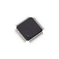
IC CODEC STEREO AUDIO 48-LQFP
Manufacturer
Cirrus Logic Inc
Type
Audio Codecr
Datasheet
1.CS42325-CQZR.pdf
(71 pages)
Specifications of CS42325-CQZ
Package / Case
48-LQFP
Data Interface
Serial
Resolution (bits)
24 b
Number Of Adcs / Dacs
1 / 2
Sigma Delta
Yes
Dynamic Range, Adcs / Dacs (db) Typ
95 / 100
Voltage - Supply, Analog
3.13 V ~ 3.47 V
Voltage - Supply, Digital
3.13 V ~ 3.47 V
Operating Temperature
-40°C ~ 85°C
Mounting Type
Surface Mount
Number Of Adc Inputs
1
Number Of Dac Outputs
2
Conversion Rate
96 KSPS
Interface Type
Serial (I2C, SPI)
Resolution
24 bit
Operating Supply Voltage
3.3 V
Maximum Operating Temperature
+ 85 C
Mounting Style
SMD/SMT
Minimum Operating Temperature
- 40 C
Number Of Channels
1 ADC/2 DAC
Supply Current
10 mA to 24 mA
Thd Plus Noise
- 88 dB ADC / - 90 dB DAC
Lead Free Status / RoHS Status
Lead free / RoHS Compliant
Lead Free Status / RoHS Status
Lead free / RoHS Compliant, Lead free / RoHS Compliant
Available stocks
Company
Part Number
Manufacturer
Quantity
Price
Company:

Part Number:
CS42325-CQZ
Manufacturer:
Cirrus Logic Inc
Quantity:
10 000
Company:
Part Number:
CS42325-CQZR
Manufacturer:
Cirrus Logic Inc
Quantity:
10 000


DS838A2
4.6.2
SCL
SDA
SDA
Software Mode - I²C Control Port
Software Mode is used to access the registers, allowing the CS42325 to be configured for the desired
operational modes and formats. The operation in Software Mode may be completely asynchronous with
respect to the audio sample rates. However, to avoid potential interference problems, the I²C pins should
remain static if no operation is required. Software Mode supports the I²C interface, with the CS42325 act-
ing as a slave device.
SDA is a bidirectional data line. Data is clocked into and out of the part by the clock, SCL. Pin AD0 forms
the least significant bit of the chip address and should be connected through a resistor to VL or GND as
desired. The state of the pin is sensed while the CS42325 is being reset.
The signal timings for a read and write cycle are shown in
defined as a falling transition of SDA while the clock is high. A Stop condition is a rising transition while
the clock is high. All other transitions of SDA occur while the clock is low. The first byte sent to the
CS42325 after a Start condition consists of a 7-bit chip address field and a R/W bit (high for a read, low
for a write). The upper 5 bits of the 7-bit address field are fixed at 10011. To communicate with a CS42325,
the chip address field, which is the first byte sent to the CS42325, should match 10011 followed by the
settings of AD0. The eighth bit of the address is the R/W bit. If the operation is a write, the next byte is the
Memory Address Pointer (MAP) which selects the register to be read or written. If the operation is a read,
the contents of the register pointed to by the MAP will be output. Setting the auto increment bit in MAP
allows successive reads or writes of consecutive registers. Each byte is separated by an acknowledge
bit. The ACK bit is output from the CS42325 after each input byte is read, and is input to the CS42325
from the microcontroller after each transmitted byte.
Since the read operation can not set the MAP, an aborted write operation is used as a preamble. As
shown in
stop condition. The following pseudocode illustrates an aborted write operation followed by a read oper-
ation.
SCL
START
START
0
1
Figure
CHIP ADDRESS (WRITE)
0
1
CHIP ADDRESS (WRITE)
1
0
1
0
0
2
2
0
1
3
21, the write operation is aborted after the acknowledge for the MAP byte by sending a
1 AD1 AD0 0
1
4
3
1 AD1 AD0 0
5
4
6
5
7
6
Figure 20. Software Mode Timing, I²C Write
ACK
Figure 21. Software Mode Timing, I²C Read
8
7
9
INCR
ACK
10 11
8
6
INCR
9
5
MAP BYTE
12 13 14 15
10 11
6
4
MAP BYTE
5
3
12
2
4
1
13 14 15
3
16
0
ACK
2
STOP
17 18
START
1
16 17 18
0
19
ACK
1
20 21 22 23 24
CHIP ADDRESS (READ)
0
7
Figure 20
0
19
6
DATA
1
1 AD1 AD0 1
24 25
1
0
25
and
ACK
26
26 27 28
ACK
27 28
7
Figure
DATA +1
7
6
DATA
0
1
21. A Start condition is
ACK
0
DATA +1
7
7
0
DATA +n
6
CS42325
DATA + n
7
1
0
0
ACK
ACK
NO
STOP
STOP
41
Related parts for CS42325-CQZ
Image
Part Number
Description
Manufacturer
Datasheet
Request
R

Part Number:
Description:
IC 10In, 6Out, 2Vrms Audio Codec WHP
Manufacturer:
Cirrus Logic Inc
Datasheet:
Part Number:
Description:
Development Kit
Manufacturer:
Cirrus Logic Inc
Datasheet:
Part Number:
Description:
Development Kit
Manufacturer:
Cirrus Logic Inc
Datasheet:


Part Number:
Description:
High-efficiency PFC + Fluorescent Lamp Driver Reference Design
Manufacturer:
Cirrus Logic Inc
Datasheet:
Part Number:
Description:
Development Kit
Manufacturer:
Cirrus Logic Inc
Datasheet:
Part Number:
Description:
Development Kit
Manufacturer:
Cirrus Logic Inc
Datasheet:

Part Number:
Description:
Development Kit
Manufacturer:
Cirrus Logic Inc
Datasheet:
Part Number:
Description:
Development Kit
Manufacturer:
Cirrus Logic Inc
Datasheet:
Part Number:
Description:
Development Kit
Manufacturer:
Cirrus Logic Inc
Datasheet:

Part Number:
Description:
EVALUATION BOARD FOR CS8427
Manufacturer:
Cirrus Logic Inc
Datasheet:

Part Number:
Description:
BOARD EVAL FOR CS8416 RCVR
Manufacturer:
Cirrus Logic Inc
Datasheet:

Part Number:
Description:
EVALUATION BOARD FOR CS8420
Manufacturer:
Cirrus Logic Inc
Datasheet:

Part Number:
Description:
KIT DEVELOPMENT EP9315 ARM9
Manufacturer:
Cirrus Logic Inc
Datasheet:

Part Number:
Description:
KIT DEVELOPMENT EP9302 ARM9
Manufacturer:
Cirrus Logic Inc
Datasheet: