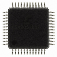
CS4205-KQZ Cirrus Logic Inc, CS4205-KQZ Datasheet - Page 74

CS4205-KQZ
Manufacturer Part Number
CS4205-KQZ
Description
IC CODEC AC97 I2S 48-LQFP
Manufacturer
Cirrus Logic Inc
Type
Audio Codec '97r
Datasheet
1.CS4205-KQZ.pdf
(81 pages)
Specifications of CS4205-KQZ
Package / Case
48-LQFP
Data Interface
Serial
Resolution (bits)
18, 20 b
Number Of Adcs / Dacs
1 / 2
Sigma Delta
Yes
Dynamic Range, Adcs / Dacs (db) Typ
90 / 90
Voltage - Supply, Analog
4.75 V ~ 5.25 V
Voltage - Supply, Digital
4.75 V ~ 5.25 V
Operating Temperature
0°C ~ 70°C
Mounting Type
Surface Mount
Number Of Adc Inputs
8
Number Of Dac Outputs
3
Conversion Rate
48 KSPs
Interface Type
Serial (5-Wire)
Resolution
18 bit, 20 bit
Maximum Operating Temperature
+ 70 C
Mounting Style
SMD/SMT
Minimum Operating Temperature
0 C
Number Of Channels
1 ADC, 1 DAC
Lead Free Status / RoHS Status
Lead free / RoHS Compliant
Other names
598-1182
Available stocks
Company
Part Number
Manufacturer
Quantity
Price
Company:
Part Number:
CS4205-KQZ
Manufacturer:
Vishay
Quantity:
718
Company:
Part Number:
CS4205-KQZR
Manufacturer:
Cirrus Logic Inc
Quantity:
10 000
Clock and Configuration Pins
XTL_IN - Crystal Input / Clock Input, Pin 2
XTL_OUT - Crystal Output / PLL Loop Filter, Pin 3
ID1#, ID0# - Codec ID, Inputs, Pins 45 and 46
Misc. Digital Interface Pins
SPDO/SDO2 - Sony/Philips Digital Interface / Serial Data Output 2, Output, Pin 48
EAPD/SCLK - External Amplifier Powerdown / Serial Clock, Output, Pin 47
GPIO0/LRCLK - General Purpose I/O / Left-Right Clock, Input/Output, Pin 43
GPIO1/SDOUT - General Purpose I/O / Serial Data Output, Input/Output, Pin 44
74
This pin requires either a 24.576 MHz crystal, with the other pin attached to XTL_OUT, or an external
CMOS clock. XTL_IN must have a crystal or clock source attached for proper operation except when
operating in secondary codec mode. The crystal frequency must be 24.576 MHz and designed for
fundamental mode, parallel resonance operation. If an external CMOS clock is used to drive this pin, it
must run at one of these acceptable frequencies: 14.31818, 24.576, 27, or 48 MHz. When configured as
a secondary codec, all timing is derived from the BIT_CLK input signal and this pin should be left
floating. See Section 11, Clocking, for additional details.
This pin is used for a crystal placed between this pin and XLT_IN. If an external 24.576 MHz clock is
used on XTL_IN, this pin must be left floating with no traces or components connected to it. If one of
the other acceptable clocks is used on XTL_IN, this pin must be connected to a loop filter circuit. See
Section 11, Clocking, for additional details.
These pins select the Codec ID for the CS4205, as well as determine the rate of the incoming clock in
PLL mode. They are only sampled after the rising edge of RESET#. These pins are internally pulled up
to the digital supply voltage and should be left floating for logic ‘0’ or tied to digital ground for logic ‘1’.
This pin generates the S/PDIF digital output from the CS4205 when the SPEN bit in the S/PDIF Control
Register (Index 68h) is ‘set’. This output may be used to directly drive a resistive divider and coupling
transformer to an RCA-type connector for use with consumer audio equipment. This pin also provides
the serial data for the second serial data port when the SDO2 bit in the Serial Port Control Register
(Index 6Ah) is ‘set’. These two functions are mutually exclusive. When neither function is being used
this output is driven to a logic ‘0’.
This pin is used to control the powerdown state of an audio amplifier external to the CS4205. The
output is controlled by the EAPD bit in the Powerdown Ctrl/Stat Register (Index 26h). It is driven as a
normal CMOS output and defaults low (‘0’) upon power-up. This pin also provides the serial clock for all
serial data ports when the SDSC bit in the Serial Port Control Register (Index 6Ah) is ‘set’.
This pin is a general purpose I/O pin that can be used to interface with various external circuitry. When
configured as an input, it functions as a Schmitt triggered input with 350 mV hysteresis at 5 V and
220 mV hysteresis at 3.3 V. When configured as an output, it can function as a normal CMOS output
(4 mA drive) or as an open drain output. This pin also provides the L/R clock for all serial data ports
when the SDEN bit in the Serial Port Control Register (Index 6Ah) is ‘set’. This pin powers up in the
high impedance state for backward compatibility.
CS4205
DS489PP4


