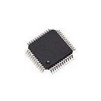
CS42324-CQZ Cirrus Logic Inc, CS42324-CQZ Datasheet - Page 36

CS42324-CQZ
Manufacturer Part Number
CS42324-CQZ
Description
IC CODEC STEREO AUDIO 48LQFP
Manufacturer
Cirrus Logic Inc
Type
Audio Codecr
Datasheet
1.CS42324-CQZ.pdf
(71 pages)
Specifications of CS42324-CQZ
Package / Case
48-LQFP
Data Interface
Serial
Resolution (bits)
24 b
Number Of Adcs / Dacs
1 / 2
Sigma Delta
Yes
Dynamic Range, Adcs / Dacs (db) Typ
95 / 100
Voltage - Supply, Analog
3.13 V ~ 3.47 V
Voltage - Supply, Digital
3.13 V ~ 3.47 V
Operating Temperature
-40°C ~ 85°C
Mounting Type
Surface Mount
Number Of Adc Inputs
1
Number Of Dac Outputs
2
Conversion Rate
96 KSPS
Interface Type
Serial (I2S, SPI)
Resolution
24 bit
Operating Supply Voltage
3.3 V
Maximum Operating Temperature
+ 85 C
Mounting Style
SMD/SMT
Minimum Operating Temperature
- 40 C
Number Of Channels
1 ADC/2 DAC
Supply Current
10 mA to 24 mA
Thd Plus Noise
- 88 dB ADC / - 90 dB DAC
Lead Free Status / RoHS Status
Lead free / RoHS Compliant
For Use With
598-1498 - BOARD EVAL FOR CS42324 CODEC
Lead Free Status / Rohs Status
Lead free / RoHS Compliant
Other names
598-1602
Available stocks
Company
Part Number
Manufacturer
Quantity
Price
Company:
Part Number:
CS42324-CQZ
Manufacturer:
TI
Quantity:
2 435
Company:
Part Number:
CS42324-CQZ
Manufacturer:
Cirrus Logic Inc
Quantity:
10 000
36
4.4.6
4.4.7
“Section 6.12 “AOUT1 Control (Address 0Dh)” on page
0Eh)” on page 57
When the device is initially powered up, the audio outputs AOUTxA and AOUTxB are clamped to VCM-
BUF which is initially low. After the PDN bit is released (set to ‘0’) the outputs begin to ramp with VCMBUF
towards the nominal quiescent voltage. This ramp takes approximately 200 ms to complete. The gradual
voltage ramping allows time for the external DC-blocking capacitors to charge to VCMBUF, effectively
blocking the quiescent DC voltage. Audio output from the DACs will begin after approximately 2000 sam-
ple periods.
To prevent audio transients at power-down, the DC-blocking capacitors must fully discharge before turn-
ing off the power. In order to do this, either the PDN bit should be set or the device should be reset about
250 ms before removing power. During this time, the voltage on VCMBUF and the AOUTx outputs dis-
charge gradually to GND. If power is removed before this 250 ms time period has passed, a transient will
occur when the VA supply drops below that of VCMBUF. There is no minimum time for a power cycle;
power may be re-applied at any time.
Analog Output Multiplexer
The CS42324 contains three independent stereo 7-to-1 analog output multiplexers which can select one
of seven possible stereo analog output sources and route it to the AOUTxA and AOUTxB pins.
shows the architecture of the analog output multiplexer.
Output Transient Control
The CS42324 uses Popguard technology to minimize the effects of output transients during power-up and
power-down. This technique eliminates the audio transients commonly produced by single-ended single-
supply converters when it is implemented with external DC-blocking capacitors connected in series with
the audio outputs. To make best use of this feature, it is necessary to understand its operation.
4.4.7.1
4.4.7.2
Power-Up
Power-Down
outline the bit settings necessary to control the output multiplexer.
Figure 18. Analog Output Architecture
DAC1A
DAC2A
DAC1B
DAC2B
AIN4A
AIN4B
AIN1A
AIN2A
AIN3A
AIN5A
AIN1B
AIN2B
AIN3B
AIN5B
AOUTx_SEL[2:0]
MUX
MUX
56” and
AOUTxA
AOUTxB
Section 6.13 “AOUT2 Control (Address
CS42324
DS721A6
Figure 18


