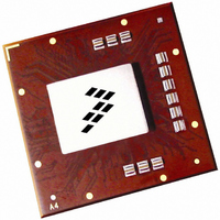
MPC8560PX833LC Freescale Semiconductor, MPC8560PX833LC Datasheet - Page 32

MPC8560PX833LC
Manufacturer Part Number
MPC8560PX833LC
Description
IC MPU PWRQUICC III 783-FCPBGA
Manufacturer
Freescale Semiconductor
Datasheet
1.MPC8560PX833LC.pdf
(104 pages)
Specifications of MPC8560PX833LC
Processor Type
MPC85xx PowerQUICC III 32-Bit
Speed
833MHz
Voltage
1.2V
Mounting Type
Surface Mount
Package / Case
783-FCPBGA
Family Name
MPC85XX
Device Core
PowerQUICC III
Device Core Size
32b
Frequency (max)
833MHz
Instruction Set Architecture
RISC
Supply Voltage 1 (typ)
1.2V
Operating Supply Voltage (max)
1.26V
Operating Supply Voltage (min)
1.14V
Operating Temp Range
0C to 105C
Operating Temperature Classification
Commercial
Mounting
Surface Mount
Pin Count
783
Package Type
FCBGA
For Use With
MPC8560ADS-BGA - BOARD APPLICATION DEV 8560
Lead Free Status / RoHS Status
Contains lead / RoHS non-compliant
Features
-
Lead Free Status / Rohs Status
Not Compliant
Available stocks
Company
Part Number
Manufacturer
Quantity
Price
Company:
Part Number:
MPC8560PX833LC
Manufacturer:
MOTOROLA
Quantity:
453
Company:
Part Number:
MPC8560PX833LC
Manufacturer:
Freescale Semiconductor
Quantity:
10 000
Part Number:
MPC8560PX833LC
Manufacturer:
FREESCALE
Quantity:
20 000
At recommended operating conditions with OV
Ethernet: Three-Speed, MII Management
7.3.2
Table 29
32
MDC frequency
MDC period
MDC clock pulse width high
MDC to MDIO valid
MDC to MDIO delay
MDIO to MDC setup time
MDIO to MDC hold time
MDC rise time
MDC fall time
Notes:
1. The symbols used for timing specifications herein follow the pattern of t
2. This parameter is dependent on the CCB clock speed (that is, for a CCB clock of 267 MHz, the maximum frequency is
3. This parameter is dependent on the CCB clock speed (that is, for a CCB clock of 267 MHz, the delay is 60 ns and for a CCB
4. Guaranteed by design.
for inputs and t
management data timing (MD) for the time t
hold time. Also, t
valid state (V) relative to the t
convention is used with the appropriate letter: R (rise) or F (fall).
8.3 MHz and the minimum frequency is 1.2 MHz; for a CCB clock of 333 MHz, the maximum frequency is 10.4 MHz and the
minimum frequency is 1.5 MHz).
clock of 333 MHz, the delay is 48 ns).
Input high current (OV
Input low current (OV
Note:
1. The symbol V
Parameter/Condition
provides the MII management AC timing specifications.
MII Management AC Electrical Specifications
(first two letters of functional block)(reference)(state)(signal)(state)
MDDVKH
IN
Table 28. MII Management DC Electrical Characteristics (continued)
, in this case, represents the OV
DD
Parameter
DD
symbolizes management data timing (MD) with respect to the time data input signals (D) reach the
MPC8560 Integrated Processor Hardware Specifications, Rev. 5
= Max, V
= Max, V
MDC
Table 29. MII Management AC Timing Specifications
clock reference (K) going to the high (H) state or setup time. For rise and fall times, the latter
IN
IN
= 0.5 V)
DD
1
Symbol
t
t
t
t
= 2.1 V)
MDKHDV
MDKHDX
MDDVKH
MDDXKH
is 3.3 V ± 5%.
t
t
t
f
t
MDCH
MDCR
MDHF
MDC
MDC
MDC
from clock reference (K) high (H) until data outputs (D) are invalid (X) or data
1
IN
symbol referenced in
0.893
Min
96
32
10
—
—
—
5
0
Symbol
I
I
IH
IL
for outputs. For example, t
(first two letters of functional block)(signal)(state) (reference)(state)
Typ
—
—
—
—
—
—
—
—
—
Table 1
–600
Min
—
and
2*[1/(f
2*[1/(f
Table
1120
Max
10.4
ccb_clk
ccb_clk
10
10
—
—
—
Max
MDKHDX
2.
40
—
/8)]
/8)]
Freescale Semiconductor
symbolizes
MHz
Unit
ns
ns
ns
ns
ns
ns
ns
ns
Unit
μA
μA
Notes
2, 4
—
—
—
—
3
3
4
4


