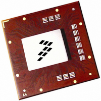
MPC8560PX833LC Freescale Semiconductor, MPC8560PX833LC Datasheet - Page 22

MPC8560PX833LC
Manufacturer Part Number
MPC8560PX833LC
Description
IC MPU PWRQUICC III 783-FCPBGA
Manufacturer
Freescale Semiconductor
Datasheet
1.MPC8560PX833LC.pdf
(104 pages)
Specifications of MPC8560PX833LC
Processor Type
MPC85xx PowerQUICC III 32-Bit
Speed
833MHz
Voltage
1.2V
Mounting Type
Surface Mount
Package / Case
783-FCPBGA
Family Name
MPC85XX
Device Core
PowerQUICC III
Device Core Size
32b
Frequency (max)
833MHz
Instruction Set Architecture
RISC
Supply Voltage 1 (typ)
1.2V
Operating Supply Voltage (max)
1.26V
Operating Supply Voltage (min)
1.14V
Operating Temp Range
0C to 105C
Operating Temperature Classification
Commercial
Mounting
Surface Mount
Pin Count
783
Package Type
FCBGA
For Use With
MPC8560ADS-BGA - BOARD APPLICATION DEV 8560
Lead Free Status / RoHS Status
Contains lead / RoHS non-compliant
Features
-
Lead Free Status / Rohs Status
Not Compliant
Available stocks
Company
Part Number
Manufacturer
Quantity
Price
Company:
Part Number:
MPC8560PX833LC
Manufacturer:
MOTOROLA
Quantity:
453
Company:
Part Number:
MPC8560PX833LC
Manufacturer:
Freescale Semiconductor
Quantity:
10 000
Part Number:
MPC8560PX833LC
Manufacturer:
FREESCALE
Quantity:
20 000
Ethernet: Three-Speed, MII Management
different than the delays seen in simulation, depending on the system topology. If a heavily loaded system
is used, the DLL loop may need to be adjusted to meet setup requirements at the DRAM.
7
This section provides the AC and DC electrical characteristics for three-speed and MII management.
7.1
The electrical characteristics specified here apply to all GMII (gigabit media independent interface), MII
(media independent interface), TBI (ten-bit interface), RGMII (reduced gigabit media independent
interface), and RTBI (reduced ten-bit interface) signals except MDIO (management data input/output) and
MDC (management data clock). The RGMII and RTBI interfaces are defined for 2.5 V, while the GMII,
MII, and TBI interfaces can be operated at 3.3 or 2.5 V. Whether the GMII, MII, or TBI interface is
operated at 3.3 or 2.5 V, the timing is compliant with the IEEE 802.3 standard. The RGMII and RTBI
interfaces follow the Hewlett-Packard reduced pin-count interface for Gigabit Ethernet Physical Layer
Device Specification Version 1.2a (9/22/2000). The electrical characteristics for MDIO and MDC are
specified in
7.1.1
All GMII,MII, TBI, RGMII, and RTBI drivers and receivers comply with the DC parametric attributes
specified in
receiver may exceed the potential of the receiver’s power supply (i.e., a GMII driver powered from a 3.6
V supply driving V
driver and receiver supply potentials is implicit in these specifications. The RGMII and RTBI signals are
based on a 2.5 V CMOS interface voltage as defined by JEDEC EIA/JESD8-5.
22
Supply voltage 3.3 V
Output high voltage (LV
Output low voltage (LV
Input high voltage
Ethernet: Three-Speed, MII Management
Three-Speed Ethernet Controller (TSEC)
(10/100/1Gb Mbps)—GMII/MII/TBI/RGMII/RTBI Electrical
Characteristics
Table 19
TSEC DC Electrical Characteristics
Section 7.3, “Ethernet Management Interface Electrical Characteristics.”
Parameter
4 devices (12 pF)
9 devices (27 pF)
36 devices (108 pF) + 40 pF compensation capacitor
36 devices (108 pF) + 80 pF compensation capacitor
OH
and
DD
DD
into a GMII receiver powered from a 2.5 V supply). Tolerance for dissimilar GMII
= Min, I
MPC8560 Integrated Processor Hardware Specifications, Rev. 5
= Min, I
Table 19. GMII, MII, and TBI DC Electrical Characteristics
Table
Table 18. Expected Delays for Address/Command
OL
OH
20. The potential applied to the input of a GMII,MII, TBI, RGMII, or RTBI
= 4.0 mA)
= –4.0 mA)
Load
Symbol
LV
V
V
V
OH
OL
IH
DD
GND
3.13
2.40
1.70
Min
Delay
3.0
3.6
5.0
5.2
LV
LV
DD
DD
Max
3.47
0.50
Unit
+ 0.3
+ 0.3
ns
ns
ns
ns
Freescale Semiconductor
Unit
V
V
V
V


