MPC850DSLZQ50BU Freescale Semiconductor, MPC850DSLZQ50BU Datasheet - Page 4
MPC850DSLZQ50BU
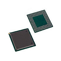
Manufacturer Part Number
MPC850DSLZQ50BU
Description
IC MPU PWRQUICC 50MHZ 256-PBGA
Manufacturer
Freescale Semiconductor
Specifications of MPC850DSLZQ50BU
Processor Type
MPC8xx PowerQUICC 32-Bit
Speed
50MHz
Voltage
3.3V
Mounting Type
Surface Mount
Package / Case
256-PBGA
Family Name
MPC8xx
Device Core
PowerQUICC
Device Core Size
32b
Frequency (max)
50MHz
Instruction Set Architecture
RISC
Supply Voltage 1 (typ)
3.3V
Operating Supply Voltage (max)
3.465V
Operating Supply Voltage (min)
3.135V
Operating Temp Range
0C to 95C
Operating Temperature Classification
Commercial
Mounting
Surface Mount
Pin Count
256
Package Type
BGA
Lead Free Status / RoHS Status
Contains lead / RoHS non-compliant
Features
-
Lead Free Status / Rohs Status
Not Compliant
Available stocks
Company
Part Number
Manufacturer
Quantity
Price

Company:
Part Number:
MPC850DSLZQ50BU
Manufacturer:
FREESCAL
Quantity:
364
Company:
Part Number:
MPC850DSLZQ50BU
Manufacturer:
Freescale Semiconductor
Quantity:
10 000
Part Number:
MPC850DSLZQ50BU
Manufacturer:
FREESCALE
Quantity:
20 000


Features
4
•
•
•
•
•
•
— 2-Kbyte instruction cache and 1-Kbyte data cache (Harvard architecture)
— Memory management units (MMUs) with 8-entry translation lookaside buffers (TLBs) and
— MMUs support multiple page sizes of 4 Kbytes, 16 Kbytes, 256 Kbytes, 512 Kbytes, and
Advanced on-chip emulation debug mode
Data bus dynamic bus sizing for 8, 16, and 32-bit buses
— Supports traditional 68000 big-endian, traditional x86 little-endian and modified little-endian
— Twenty-six external address lines
Completely static design (0–80 MHz operation)
System integration unit (SIU)
— Hardware bus monitor
— Spurious interrupt monitor
— Software watchdog
— Periodic interrupt timer
— Low-power stop mode
— Clock synthesizer
— Decrementer, time base, and real-time clock (RTC) from the PowerPC architecture
— Reset controller
— IEEE 1149.1 test access port (JTAG)
Memory controller (eight banks)
— Glueless interface to DRAM single in-line memory modules (SIMMs), synchronous DRAM
— Memory controller programmable to support most size and speed memory interfaces
— Boot chip-select available at reset (options for 8, 16, or 32-bit memory)
— Variable block sizes, 32 Kbytes to 256 Mbytes
— Selectable write protection
— On-chip bus arbiter supports one external bus master
— Special features for burst mode support
General-purpose timers
— Four 16-bit timers or two 32-bit timers
MPC850 PowerQUICC™ Integrated Communications Processor Hardware Specifications, Rev. 2
– Caches are two-way, set-associative
– Physically addressed
– Cache blocks can be updated with a 4-word line burst
– Least-recently used (LRU) replacement algorithm
– Lockable one-line granularity
fully-associative instruction and data TLBs
8 Mbytes; 16 virtual address spaces and eight protection groups
memory systems
(SDRAM), static random-access memory (SRAM), electrically programmable read-only
memory (EPROM), flash EPROM, etc.
Freescale Semiconductor
Related parts for MPC850DSLZQ50BU
Image
Part Number
Description
Manufacturer
Datasheet
Request
R

Part Number:
Description:
Connecting SP5301 to MPC850 PowerQUICC
Manufacturer:
Sipex Corporation
Datasheet:

Part Number:
Description:
Mpc850 Rev. A/b/c Communications Controller
Manufacturer:
Freescale Semiconductor, Inc
Datasheet:
Part Number:
Description:
Manufacturer:
Freescale Semiconductor, Inc
Datasheet:
Part Number:
Description:
Manufacturer:
Freescale Semiconductor, Inc
Datasheet:
Part Number:
Description:
Manufacturer:
Freescale Semiconductor, Inc
Datasheet:
Part Number:
Description:
Manufacturer:
Freescale Semiconductor, Inc
Datasheet:
Part Number:
Description:
Manufacturer:
Freescale Semiconductor, Inc
Datasheet:
Part Number:
Description:
Manufacturer:
Freescale Semiconductor, Inc
Datasheet:
Part Number:
Description:
Manufacturer:
Freescale Semiconductor, Inc
Datasheet:
Part Number:
Description:
Manufacturer:
Freescale Semiconductor, Inc
Datasheet:
Part Number:
Description:
Manufacturer:
Freescale Semiconductor, Inc
Datasheet:
Part Number:
Description:
Manufacturer:
Freescale Semiconductor, Inc
Datasheet:
Part Number:
Description:
Manufacturer:
Freescale Semiconductor, Inc
Datasheet:
Part Number:
Description:
Manufacturer:
Freescale Semiconductor, Inc
Datasheet:
Part Number:
Description:
Manufacturer:
Freescale Semiconductor, Inc
Datasheet: