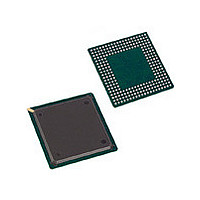
MPC850DSLZQ50BU Freescale Semiconductor, MPC850DSLZQ50BU Datasheet - Page 13

MPC850DSLZQ50BU
Manufacturer Part Number
MPC850DSLZQ50BU
Description
IC MPU PWRQUICC 50MHZ 256-PBGA
Manufacturer
Freescale Semiconductor
Specifications of MPC850DSLZQ50BU
Processor Type
MPC8xx PowerQUICC 32-Bit
Speed
50MHz
Voltage
3.3V
Mounting Type
Surface Mount
Package / Case
256-PBGA
Family Name
MPC8xx
Device Core
PowerQUICC
Device Core Size
32b
Frequency (max)
50MHz
Instruction Set Architecture
RISC
Supply Voltage 1 (typ)
3.3V
Operating Supply Voltage (max)
3.465V
Operating Supply Voltage (min)
3.135V
Operating Temp Range
0C to 95C
Operating Temperature Classification
Commercial
Mounting
Surface Mount
Pin Count
256
Package Type
BGA
Lead Free Status / RoHS Status
Contains lead / RoHS non-compliant
Features
-
Lead Free Status / Rohs Status
Not Compliant
Available stocks
Company
Part Number
Manufacturer
Quantity
Price
Company:
Part Number:
MPC850DSLZQ50BU
Manufacturer:
FREESCAL
Quantity:
364
Company:
Part Number:
MPC850DSLZQ50BU
Manufacturer:
Freescale Semiconductor
Quantity:
10 000
Part Number:
MPC850DSLZQ50BU
Manufacturer:
FREESCALE
Quantity:
20 000
Freescale Semiconductor
Num
B22a
B22b
B22c
B24a
B27a
B28a
B28b
B22
B23
B24
B25
B26
B27
B28
MPC850 PowerQUICC™ Integrated Communications Processor Hardware Specifications, Rev. 2
CLKOUT rising edge to CS
asserted GPCM ACS = 00
CLKOUT falling edge to CS
asserted GPCM ACS = 10,
TRLX = 0,1
CLKOUT falling edge to CS
asserted GPCM ACS = 11,
TRLX = 0, EBDF = 0
CLKOUT falling edge to CS
asserted GPCM ACS = 11,
TRLX = 0, EBDF = 1
CLKOUT rising edge to CS
negated GPCM read access,
GPCM write access ACS = 00,
TRLX = 0 & CSNT = 0
A[6–31] to CS asserted GPCM
ACS = 10, TRLX = 0.
A[6–31] to CS asserted GPCM
ACS = 11, TRLX = 0
CLKOUT rising edge to OE,
WE[0–3] asserted
CLKOUT rising edge to OE
negated
A[6–31] to CS asserted GPCM
ACS = 10, TRLX = 1
A[6–31] to CS asserted GPCM
ACS = 11, TRLX = 1
CLKOUT rising edge to
WE[0–3] negated GPCM write
access CSNT = 0
CLKOUT falling edge to
WE[0–3] negated GPCM write
access TRLX = 0,1 CSNT = 1,
EBDF = 0
CLKOUT falling edge to CS
negated GPCM write access
TRLX = 0,1 CSNT = 1, ACS =
10 or ACS = 11, EBDF = 0
Characteristic
Table 6. Bus Operation Timing
23.00
28.00
5.00
5.00
7.00
2.00
3.00
8.00
2.00
5.00
Min
—
—
—
—
50 MHz
14.00 11.00 18.00
12.00
12.00
11.75
11.75
Max
8.00
8.00
9.00
9.00
9.00
—
—
—
—
13.00
36.00
43.00
7.58
7.58
2.00
6.00
2.00
8.00
Min
—
—
—
—
66 MHz
14.33
14.33
14.00
14.00
Max
8.00
8.00
9.00
9.00
9.00
—
—
—
—
1
(continued)
29.00
36.00
11.00
6.25
6.25
9.00
2.00
4.00
2.00
6.00
Min
—
—
—
—
80 MHz
13.00
13.00
16.00
13.00
13.00
Max
8.00
8.00
9.00
9.00
9.00
—
—
—
—
FFACT
0.250
0.250
0.375
0.250
0.500
1.250
1.500
0.250
0.250
—
—
—
—
—
Cap Load
(default
50 pF)
50.00
50.00
50.00
50.00
50.00
50.00
50.00
50.00
50.00
50.00
50.00
50.00
50.00
50.00
Bus Signal Timing
Unit
ns
ns
ns
ns
ns
ns
ns
ns
ns
ns
ns
ns
ns
ns
13


