MPC755CRX400LE Freescale Semiconductor, MPC755CRX400LE Datasheet - Page 39
MPC755CRX400LE
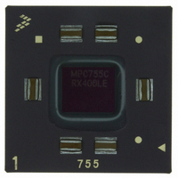
Manufacturer Part Number
MPC755CRX400LE
Description
IC MPU 32BIT 400MHZ PPC 360-CBGA
Manufacturer
Freescale Semiconductor
Datasheet
1.MPC755BPX300LE.pdf
(56 pages)
Specifications of MPC755CRX400LE
Processor Type
MPC7xx PowerPC 32-Bit
Speed
400MHz
Voltage
2V
Mounting Type
Surface Mount
Package / Case
360-FCCBGA
Family Name
MPC7xx
Device Core
PowerPC
Device Core Size
64b
Frequency (max)
400MHz
Instruction Set Architecture
RISC
Supply Voltage 1 (typ)
2V
Operating Supply Voltage (max)
2.1V
Operating Supply Voltage (min)
1.9V
Operating Temp Range
0C to 105C
Operating Temperature Classification
Commercial
Mounting
Surface Mount
Pin Count
360
Package Type
FCCBGA
Lead Free Status / RoHS Status
Contains lead / RoHS non-compliant
Features
-
Lead Free Status / Rohs Status
Not Compliant
Available stocks
Company
Part Number
Manufacturer
Quantity
Price
Company:

Part Number:
MPC755CRX400LE
Manufacturer:
MOT
Quantity:
12 388
Company:
Part Number:
MPC755CRX400LE
Manufacturer:
Freescale Semiconductor
Quantity:
10 000


These capacitors should have a value of 0.01 or 0.1 µF. Only ceramic SMT (surface mount technology)
capacitors should be used to minimize lead inductance, preferably 0508 or 0603 orientations where
connections are made along the length of the part.
In addition, it is recommended that there be several bulk storage capacitors distributed around the PCB,
feeding the V
These bulk capacitors should have a low ESR (equivalent series resistance) rating to ensure the quick
response time necessary. They should also be connected to the power and ground planes through two vias
to minimize inductance. Suggested bulk capacitors:100–330 µF (AVX TPS tantalum or Sanyo OSCON).
8.4
To ensure reliable operation, it is highly recommended to connect unused inputs to an appropriate signal
level through a resistor. Unused active low inputs should be tied to OV
should be connected to GND. All NC (no connect) signals must remain unconnected.
Power and ground connections must be made to all external V
MPC755. Note that power must be supplied to L2OV
be used; it is recommended to connect L2OV
unused. (This requirement does not apply to the MPC745 since it has neither an L2 interface nor L2OV
pins.)
8.5
The MPC755 60x and L2 I/O drivers are characterized over process, voltage, and temperature. To measure
Z
resistor is varied until the pad voltage is (L2)OV
The output impedance is the average of two components, the resistances of the pull-up and pull-down
devices. When data is held low, SW2 is closed (SW1 is open), and R
pad equals (L2)OV
SW1 is closed (SW2 is open), and R
becomes the resistance of the pull-up devices.
Freescale Semiconductor
0
, an external resistor is connected from the chip pad to (L2)OV
Connection Recommendations
Output Buffer DC Impedance
DD
, L2OV
DD
/2. R
DD
MPC755 RISC Microprocessor Hardware Specifications, Rev. 8
N
, and OV
then becomes the resistance of the pull-down devices. When data is held high,
DD
P
is trimmed until the voltage at the pad equals (L2)OV
planes, to enable quick recharging of the smaller chip capacitors.
DD
DD
to OV
/2 (see
DD
DD
even if the L2 interface of the MPC755 will not
and L2VSEL to BVSEL if the L2 interface is
Figure
DD
, OV
DD
22).
N
or GND. Then, the value of each
DD
is trimmed until the voltage at the
DD
, L2OV
. Unused active high inputs
DD
, and GND pins of the
System Design Information
DD
/2. R
P
then
DD
39
Related parts for MPC755CRX400LE
Image
Part Number
Description
Manufacturer
Datasheet
Request
R

Part Number:
Description:
Host Processor
Manufacturer:
Motorola Semiconductor Products
Datasheet:

Part Number:
Description:
Manufacturer:
Freescale Semiconductor, Inc
Datasheet:
Part Number:
Description:
Manufacturer:
Freescale Semiconductor, Inc
Datasheet:
Part Number:
Description:
Manufacturer:
Freescale Semiconductor, Inc
Datasheet:
Part Number:
Description:
Manufacturer:
Freescale Semiconductor, Inc
Datasheet:
Part Number:
Description:
Manufacturer:
Freescale Semiconductor, Inc
Datasheet:
Part Number:
Description:
Manufacturer:
Freescale Semiconductor, Inc
Datasheet:
Part Number:
Description:
Manufacturer:
Freescale Semiconductor, Inc
Datasheet:
Part Number:
Description:
Manufacturer:
Freescale Semiconductor, Inc
Datasheet:
Part Number:
Description:
Manufacturer:
Freescale Semiconductor, Inc
Datasheet:
Part Number:
Description:
Manufacturer:
Freescale Semiconductor, Inc
Datasheet:
Part Number:
Description:
Manufacturer:
Freescale Semiconductor, Inc
Datasheet:
Part Number:
Description:
Manufacturer:
Freescale Semiconductor, Inc
Datasheet:
Part Number:
Description:
Manufacturer:
Freescale Semiconductor, Inc
Datasheet:
Part Number:
Description:
Manufacturer:
Freescale Semiconductor, Inc
Datasheet: