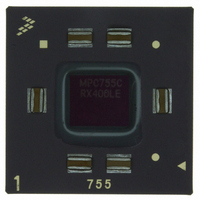
MPC755CRX400LE Freescale Semiconductor, MPC755CRX400LE Datasheet - Page 32
MPC755CRX400LE
Manufacturer Part Number
MPC755CRX400LE
Description
IC MPU 32BIT 400MHZ PPC 360-CBGA
Manufacturer
Freescale Semiconductor
Datasheet
1.MPC755BPX300LE.pdf
(56 pages)
Specifications of MPC755CRX400LE
Processor Type
MPC7xx PowerPC 32-Bit
Speed
400MHz
Voltage
2V
Mounting Type
Surface Mount
Package / Case
360-FCCBGA
Family Name
MPC7xx
Device Core
PowerPC
Device Core Size
64b
Frequency (max)
400MHz
Instruction Set Architecture
RISC
Supply Voltage 1 (typ)
2V
Operating Supply Voltage (max)
2.1V
Operating Supply Voltage (min)
1.9V
Operating Temp Range
0C to 105C
Operating Temperature Classification
Commercial
Mounting
Surface Mount
Pin Count
360
Package Type
FCCBGA
Lead Free Status / RoHS Status
Contains lead / RoHS non-compliant
Features
-
Lead Free Status / Rohs Status
Not Compliant
Available stocks
Company
Part Number
Manufacturer
Quantity
Price
Company:

Part Number:
MPC755CRX400LE
Manufacturer:
MOT
Quantity:
12 388
Company:
Part Number:
MPC755CRX400LE
Manufacturer:
Freescale Semiconductor
Quantity:
10 000


Package Description
7
The following sections provide the package parameters and mechanical dimensions for the MPC745, 255
PBGA package, as well as the MPC755, 360 CBGA and PBGA packages. While both the MPC755 plastic
and ceramic packages are described here, both packages are not guaranteed to be available at the same
time. All new designs should allow for either ceramic or plastic BGA packages for this device. For more
information on designing a common footprint for both plastic and ceramic package types, see the
Freescale Flip-Chip Plastic Ball Grid Array Presentation. The MPC755 was initially sampled in a CBGA
package, but production units are currently provided in both a CBGA and a PBGA package. Because of
the better long-term device-to-board interconnect reliability of the PBGA package, Freescale recommends
use of a PBGA package except where circumstances dictate use of a CBGA package.
32
VOLTDET
Notes:
1. OV
2. These are test signals for factory use only and must be pulled up to OV
3. This pin must be pulled up to OV
4. These pins are reserved for potential future use as additional L2 address pins.
5. Uses one of nine existing no connects in the MPC750, 360 BGA package.
6. Internal pull-up on die.
7. This pin must be pulled up to L2OV
8. Internally tied to L2OV
L2ZZ); L2OV
the L2 control signals; and V
and L2AV
selected by the BVSEL/L2VSEL pin configurations of
or supply voltages, see
provide the option to connect BVSEL independently to either OV
provide the option to connect L2VSEL independently to either L2OV
signal is not a power supply input.
Caution: This differs from the MPC745, 255 BGA package.
Signal Name
DD
Package Description
supplies power to the processor bus, JTAG, and all control signals except the L2 cache controls (L2CE, L2WE, and
DD
, respectively). These columns serve as a reference for the nominal voltage supported on a given signal as
DD
supplies power to the L2 cache interface (L2ADDR[0:16], L2DATA[0:63], L2DP[0:7], and L2SYNC_OUT) and
Table 15. Pinout Listing for the MPC755, 360 BGA Package (continued)
K13
DD
Table
in the MPC755, 360 BGA package to indicate the power present at the L2 cache interface. This
MPC755 RISC Microprocessor Hardware Specifications, Rev. 8
DD
3.
supplies power to the processor core and the PLL and DLL (after filtering to become AV
DD
DD
for proper operation of the processor interface. To allow for future I/O voltage changes,
for proper operation of the processor interface. To allow for future I/O voltage changes,
Pin Number
Table 2
and the voltage supplied. For actual recommended value of V
DD
or GND.
DD
DD
or GND.
for normal machine operation.
Active
High
Output
I/O
Freescale Semiconductor
I/F Voltage
L2OV
DD
1
Notes
8
DD
in
Related parts for MPC755CRX400LE
Image
Part Number
Description
Manufacturer
Datasheet
Request
R

Part Number:
Description:
Host Processor
Manufacturer:
Motorola Semiconductor Products
Datasheet:

Part Number:
Description:
Manufacturer:
Freescale Semiconductor, Inc
Datasheet:
Part Number:
Description:
Manufacturer:
Freescale Semiconductor, Inc
Datasheet:
Part Number:
Description:
Manufacturer:
Freescale Semiconductor, Inc
Datasheet:
Part Number:
Description:
Manufacturer:
Freescale Semiconductor, Inc
Datasheet:
Part Number:
Description:
Manufacturer:
Freescale Semiconductor, Inc
Datasheet:
Part Number:
Description:
Manufacturer:
Freescale Semiconductor, Inc
Datasheet:
Part Number:
Description:
Manufacturer:
Freescale Semiconductor, Inc
Datasheet:
Part Number:
Description:
Manufacturer:
Freescale Semiconductor, Inc
Datasheet:
Part Number:
Description:
Manufacturer:
Freescale Semiconductor, Inc
Datasheet:
Part Number:
Description:
Manufacturer:
Freescale Semiconductor, Inc
Datasheet:
Part Number:
Description:
Manufacturer:
Freescale Semiconductor, Inc
Datasheet:
Part Number:
Description:
Manufacturer:
Freescale Semiconductor, Inc
Datasheet:
Part Number:
Description:
Manufacturer:
Freescale Semiconductor, Inc
Datasheet:
Part Number:
Description:
Manufacturer:
Freescale Semiconductor, Inc
Datasheet: