MPC755CRX400LE Freescale Semiconductor, MPC755CRX400LE Datasheet - Page 18
MPC755CRX400LE
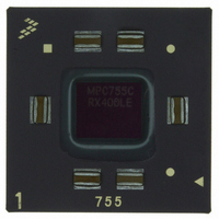
Manufacturer Part Number
MPC755CRX400LE
Description
IC MPU 32BIT 400MHZ PPC 360-CBGA
Manufacturer
Freescale Semiconductor
Datasheet
1.MPC755BPX300LE.pdf
(56 pages)
Specifications of MPC755CRX400LE
Processor Type
MPC7xx PowerPC 32-Bit
Speed
400MHz
Voltage
2V
Mounting Type
Surface Mount
Package / Case
360-FCCBGA
Family Name
MPC7xx
Device Core
PowerPC
Device Core Size
64b
Frequency (max)
400MHz
Instruction Set Architecture
RISC
Supply Voltage 1 (typ)
2V
Operating Supply Voltage (max)
2.1V
Operating Supply Voltage (min)
1.9V
Operating Temp Range
0C to 105C
Operating Temperature Classification
Commercial
Mounting
Surface Mount
Pin Count
360
Package Type
FCCBGA
Lead Free Status / RoHS Status
Contains lead / RoHS non-compliant
Features
-
Lead Free Status / Rohs Status
Not Compliant
Available stocks
Company
Part Number
Manufacturer
Quantity
Price
Company:

Part Number:
MPC755CRX400LE
Manufacturer:
MOT
Quantity:
12 388
Company:
Part Number:
MPC755CRX400LE
Manufacturer:
Freescale Semiconductor
Quantity:
10 000


Electrical and Thermal Characteristics
18
At recommended operating conditions (see
L2CLK frequency
L2CLK cycle time
L2CLK duty cycle
Internal DLL-relock time
DLL capture window
L2CLK_OUT output-to-output skew
L2CLK_OUT output jitter
Notes:
1. L2CLK outputs are L2CLK_OUTA, L2CLK_OUTB, L2CLK_OUT, and L2SYNC_OUT pins. The L2CLK frequency-to-core
2. The nominal duty cycle of the L2CLK is 50% measured at midpoint voltage.
3. The DLL-relock time is specified in terms of L2CLK periods. The number in the table must be multiplied by the period of
4. The L2CR[L2SL] bit should be set for L2CLK frequencies less than 110 MHz. This adds more delay to each tap of the DLL.
5. Allowable skew between L2SYNC_OUT and L2SYNC_IN.
6. This output jitter number represents the maximum delay of one tap forward or one tap back from the current DLL tap as the
7. Guaranteed by design.
frequency settings must be chosen such that the resulting L2CLK frequency and core frequency do not exceed their
respective maximum or minimum operating frequencies. The maximum L2LCK frequency will be system dependent.
L2CLK_OUTA and L2CLK_OUTB must have equal loading.
L2CLK to compute the actual time duration in ns. Relock timing is guaranteed by design and characterization.
phase comparator seeks to minimize the phase difference between L2SYNC_IN and the internal L2CLK. This number must
be comprehended in the L2 timing analysis. The input jitter on SYSCLK affects L2CLK_OUT and the L2 address/data/control
signals equally and, therefore, is already comprehended in the AC timing and does not have to be considered in the L2 timing
analysis.
Parameter
MPC755 RISC Microprocessor Hardware Specifications, Rev. 8
Table 11. L2CLK Output AC Timing Specification
Table
3)
t
CHCL
Symbol
t
L2CSKW
f
t
L2CLK
L2CLK
/t
L2CLK
All Speed Grades
Min
640
2.5
80
45
—
—
0
±150
Max
12.5
450
55
10
50
—
Freescale Semiconductor
L2CLK
MHz
Unit
ns
ns
ps
ps
%
Notes
1, 4
2, 7
3, 7
5, 7
6, 7
6, 7
Related parts for MPC755CRX400LE
Image
Part Number
Description
Manufacturer
Datasheet
Request
R

Part Number:
Description:
Host Processor
Manufacturer:
Motorola Semiconductor Products
Datasheet:

Part Number:
Description:
Manufacturer:
Freescale Semiconductor, Inc
Datasheet:
Part Number:
Description:
Manufacturer:
Freescale Semiconductor, Inc
Datasheet:
Part Number:
Description:
Manufacturer:
Freescale Semiconductor, Inc
Datasheet:
Part Number:
Description:
Manufacturer:
Freescale Semiconductor, Inc
Datasheet:
Part Number:
Description:
Manufacturer:
Freescale Semiconductor, Inc
Datasheet:
Part Number:
Description:
Manufacturer:
Freescale Semiconductor, Inc
Datasheet:
Part Number:
Description:
Manufacturer:
Freescale Semiconductor, Inc
Datasheet:
Part Number:
Description:
Manufacturer:
Freescale Semiconductor, Inc
Datasheet:
Part Number:
Description:
Manufacturer:
Freescale Semiconductor, Inc
Datasheet:
Part Number:
Description:
Manufacturer:
Freescale Semiconductor, Inc
Datasheet:
Part Number:
Description:
Manufacturer:
Freescale Semiconductor, Inc
Datasheet:
Part Number:
Description:
Manufacturer:
Freescale Semiconductor, Inc
Datasheet:
Part Number:
Description:
Manufacturer:
Freescale Semiconductor, Inc
Datasheet:
Part Number:
Description:
Manufacturer:
Freescale Semiconductor, Inc
Datasheet: