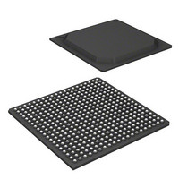
KSZ8692PBI Micrel Inc, KSZ8692PBI Datasheet - Page 34

KSZ8692PBI
Manufacturer Part Number
KSZ8692PBI
Description
IC ARM9 PHY 10/100MBPS 400-PBGA
Manufacturer
Micrel Inc
Datasheet
1.KSZ8692PBI.pdf
(42 pages)
Specifications of KSZ8692PBI
Applications
Networking & Communications
Core Processor
ARM9
Program Memory Type
External Program Memory
Controller Series
KSZ
Interface
EBI/EMI, Ethernet, I²C, I²S,PCI, SPI, UART/USART, USB
Number Of I /o
20
Voltage - Supply
1.235 V ~ 1.365 V
Operating Temperature
-40°C ~ 85°C
Mounting Type
Surface Mount
Package / Case
400-BGA
Operating Temp Range
-40C to 85C
Operating Temperature Classification
Industrial
Package Type
BGA
Mounting
Surface Mount
Lead Free Status / RoHS Status
Lead free / RoHS Compliant
Ram Size
-
Lead Free Status / RoHS Status
Supplier Unconfirmed, Lead free / RoHS Compliant
Other names
576-3627
KSZ8692PBI
KSZ8692PBI
Power-Up Strapping Options
Certain pins are sampled upon power up or reset to initialize KSZ8692PB system registers per system configuration
requirements.
Micrel, Inc.
March 2010
Pin Number
E1, E2
G1
G2
G4
G3
E3
F4
F5
F3
F2
F1
SADDR[2:1]
SADDR[10]
SADDR[11]
Pin Name
SADDR[0]
SADDR[3]
SADDR[4]
SADDR[5]
SADDR[6]
SADDR[7]
SADDR[8]
SADDR[9]
Pin Type
Ipd/O
Ipd/O
Ipd/O
Ipd/O
Ipu/O
Ipd/O
Ipd/O
Ipd/O
Ipd/O
Ipd/O
Ipd/O
Pin Description
During reset, this pin is input strap option for NAND Boot small page size
0 = 512 Bytes (default)
1 = 528 Bytes
During reset, this pin is input strap option for NAND Flash configuration register
(0x8054) bit [7:6]. These pins are used to specify number of active banks (CE#) in
cascade.
00 = 1 bank (default)
01 = 2 banks
During reset, this pin is input strap option for NAND Flash configuration register
(0x8054) bit [8], NAND Flash type. This pin is used to specify using large or small
block NAND Flash as a boot bank as follows:
“0” = small block (default)
“1” = large block
During reset, this pin is input strap option for NAND Flash configuration register
(0x8054) bit [4], NAND Flash type. This pin is used to specify number of NAND
Flash in parallel for combined data width as follows:
“0” = 1 NAND Flash (default)
“1” = 2 NAND Flash
During reset, this is input strap option to enter ARM9 tic test mode
0: ARM tic test mode (factory reserved)
1: Normal mode (default)
During reset, this pin is input strap option for NAND FLASH device support
automatic page crossing
0: NAND FLASH device does not support automatic page crossing (default)
1: NAND FLASH device supports automatic page crossing
During reset, this pin is a strapping option for B0SIZE, Bank 0 Data Access Size.
This is applicable to ROM/SRAM/FLASH and NAND boot bank.
Bank 0 is used for boot program. This pin is used to specify the size of the bank 0
data bus width as follow:
“0” = one byte (default)
“1” = half word
During reset, this pin is a strapping option for BTSEL:
“0” = Boot select from NOR flash (default)
“1” = Boot select from NAND flash
“0” = Use systems PLL (default)
“1” = Bypass systems PLL, use external clock (factory reserved)
During reset this pin is a strapping option for BYP_CLKSEL:
“0” = Select 200MHz external clock (default)
“1” = Select 250MHz external clock (factory reserved)
During reset, this pin is input strap option to enable MII mode at port1 (LAN port)
0: MII mode (default)
1: Factory Reserved
During reset this pin is a strapping option for BYP_SYSPLL:
34
M9999-031810-4.0
KSZ8692PB


