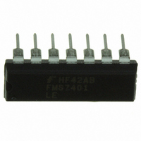
FMS7401LEN14 Fairchild Semiconductor, FMS7401LEN14 Datasheet - Page 33

FMS7401LEN14
Manufacturer Part Number
FMS7401LEN14
Description
IC CTRLR POWER DGTL EEPROM 14DIP
Manufacturer
Fairchild Semiconductor
Datasheet
1.FMS7401LVN.pdf
(81 pages)
Specifications of FMS7401LEN14
Applications
Digital Power Controller
Core Processor
8-Bit
Program Memory Type
EEPROM (1 kB)
Ram Size
64 x 8
Number Of I /o
8
Voltage - Supply
2.7 V ~ 3.6 V
Operating Temperature
-40°C ~ 85°C
Mounting Type
Through Hole
Package / Case
14-DIP (0.300", 7.62mm)
Output Current
5 mA
Input Voltage
2.7 V to 3.6 V
Switching Frequency
2 MHz
Operating Temperature Range
- 40 C to + 85 C
Mounting Style
Through Hole
Lead Free Status / RoHS Status
Lead free / RoHS Compliant
Interface
-
Controller Series
-
Lead Free Status / Rohs Status
Lead free / RoHS Compliant
Other names
FMS7401LEN14_NL
FMS7401LEN14_NL
FMS7401LEN14_NL
Available stocks
Company
Part Number
Manufacturer
Quantity
Price
Company:
Part Number:
FMS7401LEN14
Manufacturer:
Rohm
Quantity:
21 626
Bit 4 of the PSCALE register is the frequency selection (FSEL) bit for the Timer 1 circuit. FSEL is used to select between the
slow or high frequency options, ultimately selecting the F
If FSEL=0, the slow frequency option is selected and the F
determined by the FMODE bit, as discussed later in the section. If FSEL=1, the high frequency option is selected and the
F
enabled (PLLEN=0) or changed while the Timer 1 circuit is in run mode. Any attempts to write to FSEL under this condition
will be ignored and its value will remain unchanged.
Bit 3 (FMODE) of the PSCALE register is the frequency selection bit for the main instruction clock (F
to select between the slow or high frequency options, ultimately selecting the F
tor (or the external digital clock) operating at F
option is selected and the internal oscillator will then source the F
option is selected and the F
enabled, it is possible to execute instructions at a speed approximately eight times faster than the standard. The FMODE bit
may not be set if the PLL is not enabled (PLLEN=0). Any attempts to write to FMODE while PLLEN=0 will force FMODE=0
ignoring any set instructions. Once the PLL has been enabled, software may change F
normal instruction execution in order to speed-up a particular action.
Bits 2-0 of the PSCALE register are the three prescaler (PS[2:0]) bits used to divide the F
range on the PWM output signals (see
frequency equal to F
the Timer 1 circuit is in run mode, the PS value will not change the prescale division factor until after the TMR1 counter over-
flows ending the current PWM cycle. The last PS value at the TMR1 counter overflow will dictate the prescale divide factor of
the F
necessarily reflect the divide factor for the current PWM cycle.
Table 12. Prescale (PSCALE) Register Bit Definitions
Table 13. PLL Divide Factor Selection Bits and the F
REV. 1.0.3 1/24/05
PRODUCT SPECIFICATION
PWMCLK
Bit
PLLEN
FS[1:0]
FSEL
FMODE
PS[2:0]
FS[1:0]
0
0
1
1
PLLEN
T1CLK
Bit 7
0
1
0
1
will then source the F
for the next PWM cycle. When reading PS, the value reported will be the last value written by software and may not
F
16 MHz
32 MHz
64 MHz
8 MHz
PWMCLK
Description
(0) Disables the PLL circuit.
(1) Enables the PLL circuit.
PLL Divide Factor Selection Bits. Refer to
(0) Selects F
(1) Selects F
(0) Selects F
(1) Selects F
Timer 1 Prescale Selection Bits. Refer to
T1CLK
Bit 6
divided-by 1 through 8. The PS bits (like FS) may be changed by software at any time; however, if
(FS=0)
FS[1:0]
ICLK
PWMCLK
CLK
(FS=0)
FMODE=0
T1CLK
1 MHz
1 MHz
1 MHz
1 MHz
divided-by-2 output as the main system instruction clock (F
as Timer 1’s clock (F
will then source the F
PLL output as the main system instruction clock (F
PLL output as Timer 1’s clock (F
(FSEL=0)
at a frequency selected by the FS[1:0] bits. The FSEL bit may not be set if the PLL is not
Bit 5
F
Table
T1CLK
FMODE=1
14). The PS bits are used by the Timer 1 circuit to increment the 12-bit TMR1 at a
8 MHz
8 MHz
8 MHz
8 MHz
OSC
PSCALE Register (addr. 0xA4)
2
T1CLK
or the PLL’s F
FSEL
Bit 4
Table 13
ICLK
Table 13
) source.
(FSEL=1)
T1CLK
16 MHz
32 MHz
64 MHz
8 MHz
F
ICLK
with PLL’s divide-by-8 output frequency. With the FMODE bit
T1CLK
T1CLK
for details.
for details.
will then source the F
to be sourced either by the F
T1CLK
ICLK
(FS=0)
FMODE
Resolution (F
) source.
Bit 3
at a F
FMODE=0
3.906 kHz
3.906 kHz
3.906 kHz
3.906 kHz
output signal.
FSEL=0
(8-bit resolution)
OSC
Max PWM Freq.
ICLK
/2 frequency. If FMODE=1, the high frequency
ICLK
) source.
to be sourced either by the internal oscilla-
OSC
ICLK
Bit 2
T1CLK
3
31.25 kHz
ICLK
62.5 kHz
FSEL=1
125 kHz
250 kHz
If FMODE=0, the slow frequency
) source.
=2 MHz)
T1CLK
’s clock source on-the-fly during
with either a 1/8MHz frequency
ICLK
to obtain a wider frequency
or F
PS[2:0]
Bit 1
FMODE=0
244.14 Hz
244.14 Hz
244.14 Hz
244.14 Hz
FSEL=0
PWMCLK
ICLK
(12-bit resolution)
Max PWM Freq.
). FMODE is used
(see
15.625 kHz
Table
1.95 kHz
FSEL=1
Bit 0
3.9 kHz
7.8 kHz
FMS7401L
13).
33


