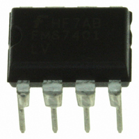
FMS7401LVN Fairchild Semiconductor, FMS7401LVN Datasheet - Page 45

FMS7401LVN
Manufacturer Part Number
FMS7401LVN
Description
IC CTRLR POWER DGTL EEPROM 8DIP
Manufacturer
Fairchild Semiconductor
Datasheet
1.FMS7401LVN.pdf
(81 pages)
Specifications of FMS7401LVN
Applications
Digital Power Controller
Core Processor
8-Bit
Program Memory Type
EEPROM (1 kB)
Ram Size
64 x 8
Number Of I /o
6
Voltage - Supply
2.7 V ~ 3.6 V
Operating Temperature
-40°C ~ 125°C
Mounting Type
Through Hole
Package / Case
8-DIP (0.300", 7.62mm)
Output Current
5 mA
Input Voltage
2.7 V to 3.6 V
Switching Frequency
2 MHz
Operating Temperature Range
- 40 C to + 125 C
Mounting Style
Through Hole
Lead Free Status / RoHS Status
Lead free / RoHS Compliant
Interface
-
Controller Series
-
Lead Free Status / Rohs Status
Lead free / RoHS Compliant
Other names
FMS7401LVN_NL
FMS7401LVN_NL
FMS7401LVN_NL
FMS7401L
The MIW circuit can be used with the I/O ports configured as both an input and output. The MIW configuration and function is
the same for both I/O configurations. However, when using the MIW circuit to wake the device from Halt/Idle Mode the
wakeup I/O port must be configured as an input, otherwise the device will never exit the mode.
Table 22. Multi-input Wakeup (MIW) Register Bit Assignments
1. Refer to the
2. Refer to
3. Hardware interrupts are not executed by the microcontroller core unless the Global Interrupt enable (G) flag of the Status register is set. Refer to the
4. No other hardware interrupts will be executed, aside from the software interrupt instruction, until the MIW hardware interrupt is no longer executed. Refer to the
5. Available only on the 14-pin package option.
6. The PWMOFF and PWMINT signals are the outputs from the Programmable Comparator’s Digital Filter circuit. Refer to
45
Microcontroller Core
8-Bit Microcontroller Core
of the datasheet for details.
PWMOFF
Bit 7
G7
G6
Table 30
5
Power Saving Modes
PWMINT
B
A
of the
PWMOFF
Sel
Y
section of the datasheet for details.
Device Memory
Bit 6
G0
section of the datasheet for details.
G7
6
/G6
section of the datasheet for detail regarding Halt and Idle Mode.
WKEDG[7:0]
5
section of the datasheet for the detailed memory map.
WKEN, WKEDG, WKPND Registers (addr. 0xB1, 0xAF, 0xB0)
Figure 15. Multi-input Wakeup (MIW) Block Diagram
Bit 5
G5
7
WKEN[7:0]
Data Bus
Bit 4
G4
0
Bit 3
G3
WKPND[7:0]
7
0
Bit 2
G2
WKINTEN
6
Programmable Comparator Circuit
PRODUCT SPECIFICATION
Bit 1
G1
REV. 1.0.3 1/24/05
WAKEOUT
EDGEI
Bit 0
G0
8-Bit
section


