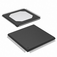
XC3S50AN-4TQG144I Xilinx Inc, XC3S50AN-4TQG144I Datasheet - Page 25

XC3S50AN-4TQG144I
Manufacturer Part Number
XC3S50AN-4TQG144I
Description
IC FPGA SPARTAN-3AN50K 144-TQFP
Manufacturer
Xilinx Inc
Series
Spartan™-3ANr
Datasheets
1.XC3S50A-4VQG100C.pdf
(7 pages)
2.XC3S50AN-4TQG144C.pdf
(2 pages)
3.XC3S50AN-4TQG144C.pdf
(123 pages)
Specifications of XC3S50AN-4TQG144I
Total Ram Bits
55296
Number Of Logic Elements/cells
1584
Number Of Labs/clbs
176
Number Of I /o
108
Number Of Gates
50000
Voltage - Supply
1.14 V ~ 1.26 V
Mounting Type
Surface Mount
Operating Temperature
-40°C ~ 100°C
Package / Case
144-LQFP
No. Of Logic Blocks
176
No. Of Gates
50000
No. Of Macrocells
1584
Family Type
Spartan-3AN
No. Of Speed Grades
4
No. Of I/o's
108
Clock
RoHS Compliant
Lead Free Status / RoHS Status
Lead free / RoHS Compliant
Other names
122-1597
XC3S50AN-4TQG144I
XC3S50AN-4TQG144I
Available stocks
Company
Part Number
Manufacturer
Quantity
Price
Company:
Part Number:
XC3S50AN-4TQG144I
Manufacturer:
XILINX
Quantity:
760
Company:
Part Number:
XC3S50AN-4TQG144I
Manufacturer:
XILINX
Quantity:
54
Company:
Part Number:
XC3S50AN-4TQG144I
Manufacturer:
XILINX
Quantity:
59
Company:
Part Number:
XC3S50AN-4TQG144I
Manufacturer:
Xilinx Inc
Quantity:
10 000
Part Number:
XC3S50AN-4TQG144I
Manufacturer:
XILINX/赛灵思
Quantity:
20 000
I/O Timing
Pin-to-Pin Clock-to-Output Times
Table 21: Pin-to-Pin Clock-to-Output Times for the IOB Output Path
DS557 (v4.1) April 1, 2011
Product Specification
Notes:
1.
2.
3.
Clock-to-Output Times
T
The numbers in this table are tested using the methodology presented in
Table 10
This clock-to-output time requires adjustment whenever a signal standard other than LVCMOS25 is assigned to the Global Clock Input or a
standard other than LVCMOS25 with 12 mA drive and Fast slew rate is assigned to the data Output. If the former is true, add the appropriate
Input adjustment from
DCM output jitter is included in all measurements.
Symbol
ICKOFDCM
T
ICKOF
and
Table
When reading from the Output
Flip-Flop (OFF), the time from the
active transition on the Global
Clock pin to data appearing at the
Output pin. The DCM is in use.
When reading from OFF, the time
from the active transition on the
Global Clock pin to data appearing
at the Output pin. The DCM is not
in use.
13.
Table
Description
26. If the latter is true, add the appropriate Output adjustment from
LVCMOS25
output drive, Fast slew
rate, with DCM
LVCMOS25
output drive, Fast slew
rate, without DCM
www.xilinx.com
Spartan-3AN FPGA Family: DC and Switching Characteristics
Conditions
(2)
(2)
, 12 mA
, 12 mA
(3)
Table 30
and are based on the operating conditions set forth in
XC3S50AN
XC3S200AN
XC3S400AN
XC3S700AN
XC3S1400AN
XC3S50AN
XC3S200AN
XC3S400AN
XC3S700AN
XC3S1400AN
Device
Table
29.
Max
3.18
3.21
2.97
3.39
3.51
4.59
4.88
4.68
4.97
5.06
-5
Speed Grade
Max
3.42
3.27
3.33
3.50
3.99
5.02
5.24
5.12
5.34
5.69
-4
Units
ns
ns
ns
ns
ns
ns
ns
ns
ns
ns
25


