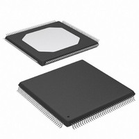
XC3S50AN-4TQG144I Xilinx Inc, XC3S50AN-4TQG144I Datasheet - Page 20

XC3S50AN-4TQG144I
Manufacturer Part Number
XC3S50AN-4TQG144I
Description
IC FPGA SPARTAN-3AN50K 144-TQFP
Manufacturer
Xilinx Inc
Series
Spartan™-3ANr
Datasheets
1.XC3S50A-4VQG100C.pdf
(7 pages)
2.XC3S50AN-4TQG144C.pdf
(2 pages)
3.XC3S50AN-4TQG144C.pdf
(123 pages)
Specifications of XC3S50AN-4TQG144I
Total Ram Bits
55296
Number Of Logic Elements/cells
1584
Number Of Labs/clbs
176
Number Of I /o
108
Number Of Gates
50000
Voltage - Supply
1.14 V ~ 1.26 V
Mounting Type
Surface Mount
Operating Temperature
-40°C ~ 100°C
Package / Case
144-LQFP
No. Of Logic Blocks
176
No. Of Gates
50000
No. Of Macrocells
1584
Family Type
Spartan-3AN
No. Of Speed Grades
4
No. Of I/o's
108
Clock
RoHS Compliant
Lead Free Status / RoHS Status
Lead free / RoHS Compliant
Other names
122-1597
XC3S50AN-4TQG144I
XC3S50AN-4TQG144I
Available stocks
Company
Part Number
Manufacturer
Quantity
Price
Company:
Part Number:
XC3S50AN-4TQG144I
Manufacturer:
XILINX
Quantity:
760
Company:
Part Number:
XC3S50AN-4TQG144I
Manufacturer:
XILINX
Quantity:
54
Company:
Part Number:
XC3S50AN-4TQG144I
Manufacturer:
XILINX
Quantity:
59
Company:
Part Number:
XC3S50AN-4TQG144I
Manufacturer:
Xilinx Inc
Quantity:
10 000
Part Number:
XC3S50AN-4TQG144I
Manufacturer:
XILINX/赛灵思
Quantity:
20 000
Table 15: Recommended Operating Conditions for User I/Os Using Differential Signal Standards (Cont’d)
Differential Output Pairs
X-Ref Target - Figure 7
DS557 (v4.1) April 1, 2011
Product Specification
Notes:
1.
2.
3.
4.
5.
6.
7.
8.
9.
DIFF_SSTL3_II
IOSTANDARD Attribute
The V
V
These true differential output standards are supported only on FPGA banks 0 and 2. Inputs are unrestricted. See the “Using I/O Resources”
chapter in UG331.
See
LVPECL is supported on inputs only, not outputs. Requires V
LVPECL_33 maximum V
Requires V
V
Table
These higher-drive output standards are supported only on FPGA banks 1 and 3. Inputs are unrestricted. See the “Using I/O Resources”
chapter in UG331.
ICM
REF
External Termination Requirements for Differential I/O, page
must be less than V
inputs are used for the DIFF_SSTL and DIFF_HSTL standards. The V
CCO
13. Other differential standards do not use V
rails supply only differential output drivers, not input circuits.
CCAUX
(8)
= 3.3V ± 10% for inputs. (V
ICM
CCAUX
Internal
Min (V)
GND level
= V
Logic
3.0
V
.
V
CCAUX
OUTN
OUTP
V
CCO
– (V
Nom (V)
for Drivers
V
3.3
OCM
V
V
V
ID
Figure 7: Differential Output Voltages
OD
OH
OL
CCAUX
/ 2)
50%
= Output common mode voltage =
= Output differential voltage =
= Output voltage indicating a High logic level
= Output voltage indicating a Low logic level
REF
– 300 mV) V
(1)
Max (V)
.
3.6
V
OCM
www.xilinx.com
CCAUX
Spartan-3AN FPGA Family: DC and Switching Characteristics
Min (mV) Nom (mV) Max (mV)
22.
100
ICM
= 3.3V ± 10%.
V
(V
V
OUTP
V
OD
OUTN
CCAUX
REF
settings are the same as for the single-ended versions in
V
V
–
ID
V
OUTP
– 37 mV)
OH
N
P
V
OUTP
- V
OUTN
Differential
I/O Pair Pins
2
+ V
DS529-3_11_082810
–
V
OUTN
OL
Min (V)
1.1
Nom (V)
V
ICM
–
(2)
Max (V)
1.9
20


