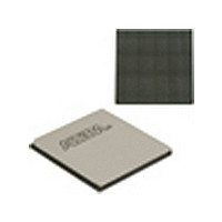
EP4SGX530HH35C2N Altera, EP4SGX530HH35C2N Datasheet - Page 69

EP4SGX530HH35C2N
Manufacturer Part Number
EP4SGX530HH35C2N
Description
IC STRATIX IV FPGA 530K 1152HBGA
Manufacturer
Altera
Series
Stratix® IV GXr
Datasheets
1.EP4SGX110DF29C3N.pdf
(80 pages)
2.EP4SGX110DF29C3N.pdf
(1154 pages)
3.EP4SGX110DF29C3N.pdf
(432 pages)
4.EP4SGX110DF29C3N.pdf
(22 pages)
5.EP4SGX110DF29C3N.pdf
(30 pages)
6.EP4SGX110DF29C3N.pdf
(72 pages)
7.EP4SGX530HH35C2N.pdf
(1145 pages)
Specifications of EP4SGX530HH35C2N
Number Of Logic Elements/cells
531200
Number Of Labs/clbs
21248
Total Ram Bits
27376
Number Of I /o
564
Voltage - Supply
0.87 V ~ 0.93 V
Mounting Type
Surface Mount
Operating Temperature
0°C ~ 85°C
Package / Case
1152-HBGA
Family Name
Stratix® IV
Number Of Logic Blocks/elements
531200
# Registers
424960
# I/os (max)
560
Process Technology
40nm
Operating Supply Voltage (typ)
900mV
Logic Cells
531200
Ram Bits
28033024
Operating Supply Voltage (min)
0.87V
Operating Supply Voltage (max)
0.93V
Operating Temp Range
0C to 85C
Operating Temperature Classification
Commercial
Mounting
Surface Mount
Pin Count
1152
Package Type
FCHBGA
Lead Free Status / RoHS Status
Lead free / RoHS Compliant
Number Of Gates
-
Lead Free Status / Rohs Status
Compliant
Available stocks
Company
Part Number
Manufacturer
Quantity
Price
Chapter 1: DC and Switching Characteristics for Stratix IV Devices
I/O Timing
I/O Timing
Table 1–51. IOE Programmable Delay for Stratix IV Devices
April 2011 Altera Corporation
Notes to
(1) You can set this value in the Quartus II software by selecting D1, D2, D3, D4, D5, and D6 in the Assignment Name column.
(2) Minimum offset does not include the intrinsic delay.
(3) For the EP4SGX530 device density, the IOE programmable delays have an additional 5% maximum offset.
Parameter
D1
D2
D3
D4
D5
D6
(1)
Table
Programmable IOE Delay
1–51:
f
Available
Settings
16
16
16
8
8
8
Duty Cycle Distortion (DCD) Specifications
Table 1–50
Table 1–50. Worst-Case DCD on Stratix IV I/O Pins
Altera offers two ways to determine I/O timing—the Excel-based I/O Timing and the
Quartus II Timing Analyzer.
Excel-based I/O Timing provides pin timing performance for each device density and
speed grade. The data is typically used prior to designing the FPGA to get an estimate
of the timing budget as part of the link timing analysis. The Quartus II Timing
Analyzer provides a more accurate and precise I/O timing data based on the specifics
of the design after you complete place-and-route.
The Excel-based I/O Timing spreadsheet is downloadable from the
Stratix IV Devices
Table 1–51
Output Duty Cycle
Min Offset
Symbol
(2)
0
0
0
0
0
0
lists the worst-case DCD for Stratix IV devices.
lists the Stratix IV IOE programmable delay settings.
Industrial
0.462
0.234
1.700
0.508
0.472
0.186
webpage.
Fast Model
Min
45
Speed Grade
–2/–2×
Commercial
0.505
0.232
1.769
0.554
0.500
0.195
(3)
Max
55
Stratix IV Device Handbook Volume 4: Device Datasheet and Addendum
C2
0.732
0.337
2.695
0.813
0.747
0.294
Min
Speed Grade
45
(3)
–3
Max
0.795
0.372
2.927
0.882
0.799
0.319
55
C3
Min
0.857
0.407
3.157
0.952
0.875
0.345
Speed Grade
45
C4
Slow Model
–4
Max
0.801
0.371
2.948
0.889
0.817
0.321
55
I3
Literature:
0.864
0.405
3.178
0.959
0.882
0.347
I4
Unit
%
1–61
Unit
ns
ns
ns
ns
ns
ns


