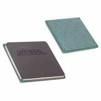
EP1SGX25DF672I6 Altera, EP1SGX25DF672I6 Datasheet - Page 156

EP1SGX25DF672I6
Manufacturer Part Number
EP1SGX25DF672I6
Description
IC STRATIX GX FPGA 25K 672-FBGA
Manufacturer
Altera
Series
Stratix® GXr
Datasheet
1.EP1SGX10CF672C7N.pdf
(272 pages)
Specifications of EP1SGX25DF672I6
Number Of Logic Elements/cells
25660
Number Of Labs/clbs
2566
Total Ram Bits
1944576
Number Of I /o
455
Voltage - Supply
1.425 V ~ 1.575 V
Mounting Type
Surface Mount
Operating Temperature
-40°C ~ 100°C
Package / Case
672-FBGA
Family Name
Stratix GX
Number Of Logic Blocks/elements
25660
# I/os (max)
455
Frequency (max)
5GHz
Process Technology
SRAM
Operating Supply Voltage (typ)
1.5V
Logic Cells
25660
Ram Bits
1944576
Operating Supply Voltage (min)
1.425V
Operating Supply Voltage (max)
1.575V
Operating Temp Range
-40C to 100C
Operating Temperature Classification
Industrial
Mounting
Surface Mount
Pin Count
672
Package Type
FC-FBGA
Lead Free Status / RoHS Status
Contains lead / RoHS non-compliant
Number Of Gates
-
Lead Free Status / Rohs Status
Not Compliant
Available stocks
Company
Part Number
Manufacturer
Quantity
Price
Company:
Part Number:
EP1SGX25DF672I6
Manufacturer:
ALTERA30
Quantity:
50
PLLs & Clock Networks
4–90
Stratix GX Device Handbook, Volume 1
■
■
Phase & Delay Shifting
Stratix GX device enhanced PLLs provide advanced programmable
phase and clock delay shifting. For phase shifting, you can specify a
phase shift (in degrees or time units) for each PLL clock output port or for
all outputs together in one shift. Phase-shifting values in time units are
allowed with a resolution range of 160 to 420 ps. This resolution is a
function of frequency input and the multiplication and division factors.
In other words, it is a function of the VCO period equal to one-eighth of
the VCO period. Each clock output counter can choose a different phase
of the VCO period from up to eight taps. You can use this clock output
counter along with an initial setting on the post-scale counter to achieve
a phase-shift range for the entire period of the output clock. The phase tap
feedback to the m counter can shift all outputs to a single phase or delay.
The Quartus II software automatically sets the phase taps and counter
settings according to the phase shift entered.
In addition to the phase-shift feature, the fine tune clock delay shift
feature provides advanced time delay shift control on each of the four
PLL outputs. Each PLL output shifts in 250-ps increments for a range of
–3.0 ns to +3.0 ns between any two outputs using discrete delay elements.
Total delay shift between any two PLL outputs must be less than 3 ns. For
example, shifts on outputs of –1 and +2 ns is allowed, but not –1 and
+2.5 ns. There is some delay variation due to process, voltage, and
temperature. Only the clock delay shift blocks can be controlled during
system operation for dynamic clock delay control.
Spread-Spectrum Clocking
The Stratix GX device’s enhanced PLLs use spread-spectrum technology
to reduce electromagnetic interference generation from a system by
distributing the energy over a broader frequency range. The enhanced
feedback for one of the dedicated external outputs, either one
single-ended or one differential pair. In this mode, one e counter
feeds back to the PLL FBIN input, becoming part of the feedback
loop.
Normal mode: If an internal clock is used in this mode, it is
phase-aligned to the input clock pin. The external clock output pin
has a phase delay relative to the clock input pin if connected in this
mode. You define which internal clock output from the PLL should
be phase-aligned to the internal clock pin.
No compensation: In this mode, the PLL does not compensate for
any clock networks or external clock outputs.
Altera Corporation
February 2005


