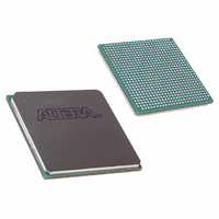
EP1SGX25DF672I6 Altera, EP1SGX25DF672I6 Datasheet - Page 134

EP1SGX25DF672I6
Manufacturer Part Number
EP1SGX25DF672I6
Description
IC STRATIX GX FPGA 25K 672-FBGA
Manufacturer
Altera
Series
Stratix® GXr
Datasheet
1.EP1SGX10CF672C7N.pdf
(272 pages)
Specifications of EP1SGX25DF672I6
Number Of Logic Elements/cells
25660
Number Of Labs/clbs
2566
Total Ram Bits
1944576
Number Of I /o
455
Voltage - Supply
1.425 V ~ 1.575 V
Mounting Type
Surface Mount
Operating Temperature
-40°C ~ 100°C
Package / Case
672-FBGA
Family Name
Stratix GX
Number Of Logic Blocks/elements
25660
# I/os (max)
455
Frequency (max)
5GHz
Process Technology
SRAM
Operating Supply Voltage (typ)
1.5V
Logic Cells
25660
Ram Bits
1944576
Operating Supply Voltage (min)
1.425V
Operating Supply Voltage (max)
1.575V
Operating Temp Range
-40C to 100C
Operating Temperature Classification
Industrial
Mounting
Surface Mount
Pin Count
672
Package Type
FC-FBGA
Lead Free Status / RoHS Status
Contains lead / RoHS non-compliant
Number Of Gates
-
Lead Free Status / Rohs Status
Not Compliant
Available stocks
Company
Part Number
Manufacturer
Quantity
Price
Company:
Part Number:
EP1SGX25DF672I6
Manufacturer:
ALTERA30
Quantity:
50
- Current page: 134 of 272
- Download datasheet (3Mb)
PLLs & Clock Networks
PLLs & Clock
Networks
4–68
Stratix GX Device Handbook, Volume 1
clock signals are routed from LAB row clocks and are generated from
specific LAB rows at the DSP block interface. The LAB row source for
control signals, data inputs, and outputs is shown in
Stratix GX devices provide a hierarchical clock structure and multiple
PLLs with advanced features. The large number of clocking resources in
combination with the clock synthesis precision provided by enhanced
and fast PLLs provides a complete clock management solution.
Stratix GX devices contain up to four enhanced PLLs and up to four fast
PLLs. In addition, there are four receiver PLLs and one transmitter PLL
per transceiver block located on the right side of Stratix GX devices.
Global & Hierarchical Clocking
Stratix GX devices provide 16 dedicated global clock networks,
16 regional clock networks (four per device quadrant), 8 dedicated fast
regional clock networks within EP1SGX10 and EP1SGX25, and 16
dedicated fast regional clock networks within EP1SGX40 devices.
1
2
3
4
5
6
7
8
Table 4–16. DSP Block Signal Sources & Destinations
LAB Row at
Interface
signa
aclr0
accum_sload0
addnsub1
clock0
ena0
aclr1
clock1
ena1
aclr2
clock2
ena2
sign_b
clock3
ena3
clear3
accum_sload1
addnsub3
Control Signals
Generated
A1[17..0]
B1[17..0]
A2[17..0]
B2[17..0]
A3[17..0]
B3[17..0]
A4[17..0]
B4[17..0]
Data Inputs
Table
Altera Corporation
OA[17..0]
OB[17..0]
OC[17..0]
OD[17..0]
OE[17..0]
OF[17..0]
OG[17..0]
OH[17..0]
Data Outputs
February 2005
4–16.
Related parts for EP1SGX25DF672I6
Image
Part Number
Description
Manufacturer
Datasheet
Request
R

Part Number:
Description:
Stratix Gx Device Family Data Sheet
Manufacturer:
Altera Corporation
Datasheet:

Part Number:
Description:
CYCLONE II STARTER KIT EP2C20N
Manufacturer:
Altera
Datasheet:

Part Number:
Description:
CPLD, EP610 Family, ECMOS Process, 300 Gates, 16 Macro Cells, 16 Reg., 16 User I/Os, 5V Supply, 35 Speed Grade, 24DIP
Manufacturer:
Altera Corporation
Datasheet:

Part Number:
Description:
CPLD, EP610 Family, ECMOS Process, 300 Gates, 16 Macro Cells, 16 Reg., 16 User I/Os, 5V Supply, 15 Speed Grade, 24DIP
Manufacturer:
Altera Corporation
Datasheet:

Part Number:
Description:
Manufacturer:
Altera Corporation
Datasheet:

Part Number:
Description:
CPLD, EP610 Family, ECMOS Process, 300 Gates, 16 Macro Cells, 16 Reg., 16 User I/Os, 5V Supply, 30 Speed Grade, 24DIP
Manufacturer:
Altera Corporation
Datasheet:

Part Number:
Description:
High-performance, low-power erasable programmable logic devices with 8 macrocells, 10ns
Manufacturer:
Altera Corporation
Datasheet:

Part Number:
Description:
High-performance, low-power erasable programmable logic devices with 8 macrocells, 7ns
Manufacturer:
Altera Corporation
Datasheet:

Part Number:
Description:
Classic EPLD
Manufacturer:
Altera Corporation
Datasheet:

Part Number:
Description:
High-performance, low-power erasable programmable logic devices with 8 macrocells, 10ns
Manufacturer:
Altera Corporation
Datasheet:

Part Number:
Description:
Manufacturer:
Altera Corporation
Datasheet:

Part Number:
Description:
Manufacturer:
Altera Corporation
Datasheet:

Part Number:
Description:
Manufacturer:
Altera Corporation
Datasheet:


