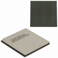
EP2SGX60EF1152C5N Altera, EP2SGX60EF1152C5N Datasheet - Page 134

EP2SGX60EF1152C5N
Manufacturer Part Number
EP2SGX60EF1152C5N
Description
IC STRATIX II GX 60K 1152-FBGA
Manufacturer
Altera
Series
Stratix® II GXr
Datasheet
1.EP2SGX30DF780C5.pdf
(316 pages)
Specifications of EP2SGX60EF1152C5N
Number Of Logic Elements/cells
60440
Number Of Labs/clbs
3022
Total Ram Bits
2544192
Number Of I /o
534
Voltage - Supply
1.15 V ~ 1.25 V
Mounting Type
Surface Mount
Operating Temperature
0°C ~ 85°C
Package / Case
1152-FBGA
Family Name
Stratix II GX
Number Of Logic Blocks/elements
60440
# I/os (max)
534
Frequency (max)
609.76MHz
Process Technology
SRAM
Operating Supply Voltage (typ)
1.2V
Logic Cells
60440
Ram Bits
2544192
Operating Supply Voltage (min)
1.15V
Operating Supply Voltage (max)
1.25V
Operating Temp Range
0C to 85C
Operating Temperature Classification
Commercial
Mounting
Surface Mount
Pin Count
1152
Package Type
FC-FBGA
Lead Free Status / RoHS Status
Lead free / RoHS Compliant
Number Of Gates
-
Lead Free Status / Rohs Status
Compliant
Other names
544-2185
Available stocks
Company
Part Number
Manufacturer
Quantity
Price
Company:
Part Number:
EP2SGX60EF1152C5N
Manufacturer:
ALTERA
Quantity:
533
Part Number:
EP2SGX60EF1152C5N
Manufacturer:
ALTERA/阿尔特拉
Quantity:
20 000
- Current page: 134 of 316
- Download datasheet (2Mb)
I/O Structure
2–126
Stratix II GX Device Handbook, Volume 1
f
The bus-hold circuitry also pulls undriven pins away from the input
threshold voltage where noise can cause unintended high-frequency
switching. You can select this feature individually for each I/O pin. The
bus-hold output drives no higher than V
signals. If the bus-hold feature is enabled, the programmable pull-up
option cannot be used. Disable the bus-hold feature when the I/O pin has
been configured for differential signals.
The bus-hold circuitry uses a resistor with a nominal resistance (RBH) of
approximately 7 kΩ to pull the signal level to the last-driven state.
Refer to the
Stratix II GX Device Handbook for the specific sustaining current driven
through this resistor and overdrive current used to identify the
next-driven input level. This information is provided for each V
voltage level.
The bus-hold circuitry is active only after configuration. When going into
user mode, the bus-hold circuit captures the value on the pin present at
the end of configuration.
Programmable Pull-Up Resistor
Each Stratix II GX device I/O pin provides an optional programmable
pull-up resistor during user mode. If you enable this feature for an I/O
pin, the pull-up resistor (typically 25 kΩ ) holds the output to the V
level of the output pin’s bank.
Programmable pull-up resistors are only supported on user I/O pins and
are not supported on dedicated configuration pins, JTAG pins, or
dedicated clock pins.
Advanced I/O Standard Support
The Stratix II GX device IOEs support the following I/O standards:
■
■
■
■
■
■
■
■
■
■
■
3.3-V LVTTL/LVCMOS
2.5-V LVTTL/LVCMOS
1.8-V LVTTL/LVCMOS
1.5-V LVCMOS
3.3-V PCI
3.3-V PCI-X mode 1
LVDS
LVPECL (on input and output clocks only)
Differential 1.5-V HSTL class I and II
Differential 1.8-V HSTL class I and II
Differential SSTL-18 class I and II
DC & Switching Characteristics
CCIO
chapter in volume 1 of the
to prevent overdriving
Altera Corporation
October 2007
CCIO
CCIO
Related parts for EP2SGX60EF1152C5N
Image
Part Number
Description
Manufacturer
Datasheet
Request
R

Part Number:
Description:
4. Serial Configuration Devices Epcs1, Epcs4, Epcs16, Epcs64, And Epcs128 Data Sheet
Manufacturer:
Altera Corporation
Datasheet:

Part Number:
Description:
CYCLONE II STARTER KIT EP2C20N
Manufacturer:
Altera
Datasheet:

Part Number:
Description:
CPLD, EP610 Family, ECMOS Process, 300 Gates, 16 Macro Cells, 16 Reg., 16 User I/Os, 5V Supply, 35 Speed Grade, 24DIP
Manufacturer:
Altera Corporation
Datasheet:

Part Number:
Description:
CPLD, EP610 Family, ECMOS Process, 300 Gates, 16 Macro Cells, 16 Reg., 16 User I/Os, 5V Supply, 15 Speed Grade, 24DIP
Manufacturer:
Altera Corporation
Datasheet:

Part Number:
Description:
Manufacturer:
Altera Corporation
Datasheet:

Part Number:
Description:
CPLD, EP610 Family, ECMOS Process, 300 Gates, 16 Macro Cells, 16 Reg., 16 User I/Os, 5V Supply, 30 Speed Grade, 24DIP
Manufacturer:
Altera Corporation
Datasheet:

Part Number:
Description:
High-performance, low-power erasable programmable logic devices with 8 macrocells, 10ns
Manufacturer:
Altera Corporation
Datasheet:

Part Number:
Description:
High-performance, low-power erasable programmable logic devices with 8 macrocells, 7ns
Manufacturer:
Altera Corporation
Datasheet:

Part Number:
Description:
Classic EPLD
Manufacturer:
Altera Corporation
Datasheet:

Part Number:
Description:
High-performance, low-power erasable programmable logic devices with 8 macrocells, 10ns
Manufacturer:
Altera Corporation
Datasheet:

Part Number:
Description:
Manufacturer:
Altera Corporation
Datasheet:

Part Number:
Description:
Manufacturer:
Altera Corporation
Datasheet:

Part Number:
Description:
Manufacturer:
Altera Corporation
Datasheet:


