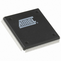
AT40K20-2EQC Atmel, AT40K20-2EQC Datasheet - Page 2

AT40K20-2EQC
Manufacturer Part Number
AT40K20-2EQC
Description
IC FPGA 20K GATES 240PQFP
Manufacturer
Atmel
Series
AT40K/KLVr
Specifications of AT40K20-2EQC
Number Of Logic Elements/cells
1024
Total Ram Bits
8192
Number Of I /o
193
Number Of Gates
30000
Voltage - Supply
4.75 V ~ 5.25 V
Mounting Type
Surface Mount
Operating Temperature
0°C ~ 70°C
Package / Case
240-BFQFP
Family Name
AT40K
Number Of Usable Gates
30000
Number Of Logic Blocks/elements
1024
# Registers
1024
# I/os (max)
193
Process Technology
0.6um (CMOS)
Operating Supply Voltage (typ)
5V
Logic Cells
1024
Ram Bits
8192
Device System Gates
30000
Operating Supply Voltage (min)
4.75V
Operating Supply Voltage (max)
5.25V
Operating Temp Range
0C to 70C
Operating Temperature Classification
Commercial
Mounting
Surface Mount
Pin Count
240
Package Type
PQFP
Lead Free Status / RoHS Status
Contains lead / RoHS non-compliant
Number Of Labs/clbs
-
Lead Free Status / Rohs Status
Not Compliant
Other names
AT40K202EQC
Available stocks
Company
Part Number
Manufacturer
Quantity
Price
Description
Fast, Flexible and
Efficient SRAM
Fast, Efficient Array and
Vector Multipliers
2
AT40K/AT40KLV Series FPGA
Table 1. AT40K/AT40KLV Family
Note:
The AT40K/AT40KLV is a family of fully PCI-compliant, SRAM-based FPGAs with dis-
tributed 10 ns programmable synchronous/asynchronous, dual-port/single-port SRAM,
8 global clocks, Cache Logic ability (partially or fully reconfigurable without loss of data),
automatic component generators, and range in size from 5,000 to 50,000 usable gates.
I/O counts range from 128 to 384 in industry standard packages ranging from 84-pin
PLCC to 352-ball Square BGA, and support 5V designs for AT40K and 3.3V designs for
AT40KLV.
The AT40K/AT40KLV is designed to quickly implement high-performance, large gate
count designs through the use of synthesis and schematic-based tools used on a PC or
Sun platform. Atmel’s design tools provide seamless integration with industry standard
tools such as Synplicity, ModelSim, Exemplar and Viewlogic.
The AT40K/AT40KLV can be used as a coprocessor for high-speed (DSP/processor-
based) designs by implementing a variety of computation intensive, arithmetic functions.
These include adaptive finite impulse response (FIR) filters, fast Fourier transforms
(FFT), convolvers, interpolators and discrete-cosine transforms (DCT) that are required
for video compression and decompression, encryption, convolution and other multime-
dia applications.
The AT40K/AT40KLV FPGA offers a patented distributed 10 ns SRAM capability where
the RAM can be used without losing logic resources. Multiple independent, synchronous
or asynchronous, dual-port or single-port RAM functions (FIFO, scratch pad, etc.) can
be created using Atmel’s macro generator tool.
The AT40K/AT40KLV’s patented 8-sided core cell with direct horizontal, vertical and
diagonal cell-to-cell connections implements ultra fast array multipliers without using
any busing resources. The AT40K/AT40KLV’s Cache Logic capability enables a large
number of design coefficients and variables to be implemented in a very small amount
of silicon, enabling vast improvement in system speed at much lower cost than conven-
tional FPGAs.
Device
Usable Gates
Rows x Columns
Cells
Registers
RAM Bits
I/O (Maximum)
1. Packages with FCK will have 8 less registers.
AT40K05LV
AT40K05
5K - 10K
16 x 16
256
2,048
256
128
(1)
(1)
AT40K10LV
10K - 20K
AT40K10
24 x 24
576
4,608
576
192
(1)
AT40K20LV
20K - 30K
AT40K20
1,024
32 x 32
1,024
8,192
256
(1)
0896C–FPGA–04/02
AT40K40LV
40K - 50K
AT40K40
2,304
48 x 48
18,432
2,304
384
(1)


