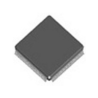
ADSP-2195MKST-160 Analog Devices Inc, ADSP-2195MKST-160 Datasheet - Page 25

ADSP-2195MKST-160
Manufacturer Part Number
ADSP-2195MKST-160
Description
IC DSP CONTROLLER 16BIT 144LQFP
Manufacturer
Analog Devices Inc
Series
ADSP-21xxr
Type
Fixed Pointr
Datasheet
1.ADSP-2195MKST-160.pdf
(68 pages)
Specifications of ADSP-2195MKST-160
Rohs Status
RoHS non-compliant
Interface
Host Interface, SPI, SSP, UART
Clock Rate
160MHz
Non-volatile Memory
ROM (48 kB)
On-chip Ram
80kB
Voltage - I/o
3.30V
Voltage - Core
2.50V
Operating Temperature
0°C ~ 70°C
Mounting Type
Surface Mount
Package / Case
144-LQFP
Device Core Size
24b
Format
Fixed Point
Clock Freq (max)
160MHz
Mips
160
Device Input Clock Speed
160MHz
Ram Size
32KB
Program Memory Size
48KB
Operating Supply Voltage (typ)
2.5/3.3V
Operating Supply Voltage (min)
2.37V
Operating Supply Voltage (max)
2.63/3.6V
Operating Temp Range
0C to 70C
Operating Temperature Classification
Commercial
Mounting
Surface Mount
Pin Count
144
Package Type
LQFP
Lead Free Status / Rohs Status
Not Compliant
Clock In and Clock Out Cycle Timing
Table 8
page
Table 8. Clock In and Clock Out Cycle Timing
1
2
3
REV. PrA
Figure 11
see the System Design chapter of the ADSP-219x/2191 DSP Hardware Reference.
In clock multiplier mode and MSEL6–0 set for 1:1 (or CLKIN=CCLK), t
In bypass mode, t
September 2001
Parameter
Switching Characteristic
t
t
Timing Requirements
t
t
t
t
t
t
CKOD
CKO
CK
CKL
CKH
WRST
MSLS
MSLH
24, combinations of CLKIN and clock multipliers must not select core/peripheral clocks in excess of 160/100 MHz.
and
shows a 2 ratio between CLKOUT = 2 CLKIN (or t
Figure 11
CK
This information applies to a product under development. Its characteristics and specifications are subject to change with-
out notice. Analog Devices assumes no obligation regarding future manufacturing unless otherwise agreed to in writing.
=t
CLKOUT delay from CLKIN
CLKOUT period
CLKIN period
CLKIN low pulse
CLKIN high pulse
RESET asserted pulsewidth low
MSELx/BYPASS stable before RESET asserted setup
MSELx/BYPASS stable after RESET de-asserted hold
CCLK
Description
.
describe clock and reset operations. Per
For current information contact Analog Devices at 800/262-5643
2,3
1
Figure 11. Clock In and Clock Out Cycle Timing
HCLK
= 2 t
CK
CCLK
=t
V
CCLK
DDINT
), but the ratio has many programmable options. For more information
.
Internal (Core) Supply Voltage, –0.3 to 3.0 V on
Min
0
10
6.25
2.2
2.2
200t
160
1000
CLKOUT
Max
5.8
200
ADSP-2195
Unit
ns
ns
ns
ns
ns
ns
µs
ns
25


