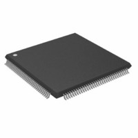
ADSP-2196MKSTZ-160 Analog Devices Inc, ADSP-2196MKSTZ-160 Datasheet - Page 21

ADSP-2196MKSTZ-160
Manufacturer Part Number
ADSP-2196MKSTZ-160
Description
IC DSP CONTROLLER 16BIT 144-LQFP
Manufacturer
Analog Devices Inc
Series
ADSP-21xxr
Type
Fixed Pointr
Datasheet
1.ADSP-2196MKSTZ-160.pdf
(68 pages)
Specifications of ADSP-2196MKSTZ-160
Interface
Host Interface, SPI, SSP, UART
Clock Rate
160MHz
Non-volatile Memory
ROM (48 kB)
On-chip Ram
40kB
Voltage - I/o
3.30V
Voltage - Core
2.50V
Operating Temperature
0°C ~ 70°C
Mounting Type
Surface Mount
Package / Case
144-LQFP
Device Core Size
16b
Format
Fixed Point
Clock Freq (max)
160MHz
Mips
160
Device Input Clock Speed
160MHz
Ram Size
40KB
Program Memory Size
48KB
Operating Supply Voltage (typ)
2.5/3.3V
Operating Supply Voltage (min)
2.37V
Operating Supply Voltage (max)
2.63/3.6V
Operating Temp Range
0C to 70C
Operating Temperature Classification
Commercial
Mounting
Surface Mount
Pin Count
144
Package Type
LQFP
Lead Free Status / RoHS Status
Lead free / RoHS Compliant
Available stocks
Company
Part Number
Manufacturer
Quantity
Price
Company:
Part Number:
ADSP-2196MKSTZ-160
Manufacturer:
Analog Devices Inc
Quantity:
10 000
Table 7. Pin Descriptions (Continued)
REV. PrA
September 2001
Pin
RCLK1–0
RCLK2/SCK1
RFS1–0
RFS2/MOSI1
TCLK1–0
TCLK2/SCK0
TFS1–0
TFS2/MOSI0
DR1–0
DR2/MISO1
DT1–0
DT2/MISO0
TMR2–0
RXD
TXD
RESET
TCK
TMS
TDI
TDO
TRST
EMU
V
V
GND
NC
DDINT
DDEXT
This information applies to a product under development. Its characteristics and specifications are subject to change with-
out notice. Analog Devices assumes no obligation regarding future manufacturing unless otherwise agreed to in writing.
Type
I/O/T
I/O/T
I/O/T
I/O/T
I/O/T
I/O/T
I/O/T
I/O/T
I/T
I/O/T
O/T
I/O/T
I/O/T
I
O
I
I
I
I
O
I
O
P
P
G
Function
SPORT1–0 Receive Clock
SPORT2 Receive Clock/SPI1 Serial Clock
SPORT1–0 Receive Frame Sync
SPORT2 Receive Frame Sync/SPI1 Master-Output, Slave-Input data
SPORT1–0 Transmit Clock
SPORT2 Transmit Clock/SPI0 Serial Clock
SPORT1–0 Transmit Frame Sync
SPORT2 Transmit Frame Sync/SPI0 Master-Output, Slave-Input data
SPORT1–0 Serial Data Receive
SPORT2 Serial Data Receive/SPI1 Master-Input, Slave-Output data
SPORT1–0 Serial Data Transmit
SPORT2 Serial Data Transmit/SPI0 Master-Input, Slave-Output data
Timer output or capture
UART Serial Receive Data
UART Serial Transmit Data
Processor Reset. Resets the ADSP-2196 to a known state and begins execution at the program
memory location specified by the hardware reset vector address. The RESET input must be
asserted (low) at power-up. The RESET pin has a 85 k internal pull-up resistor.
Test Clock (JTAG). Provides a clock for JTAG boundary scan. The TCK pin has a 85 k
internal pull-up resistor.
Test Mode Select (JTAG). Used to control the test state machine. The TMS pin has a 85 k
internal pull-up resistor.
Test Data Input (JTAG). Provides serial data for the boundary scan logic. The TDI pin has
a 85 k internal pull-up resistor.
Test Data Output (JTAG). Serial scan output of the boundary scan path.
Test Reset (JTAG). Resets the test state machine. TRST must be asserted (pulsed low) after
power-up or held low for proper operation of the ADSP-2196. The TRST pin has a 65 k
internal pull-down resistor.
Emulation Status (JTAG). Must be connected to the ADSP-2196 emulator target board
connector only.
Core Power Supply. Nominally 2.5 V dc and supplies the DSP’s core processor. (four pins).
I/O Power Supply; Nominally 3.3 V dc. (nine pins).
Power Supply Return. (twelve pins).
Do Not Connect. Reserved pins that must be left open and unconnected.
For current information contact Analog Devices at 800/262-5643
ADSP-2196
21


