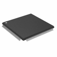
ADSP-2196MKSTZ-160 Analog Devices Inc, ADSP-2196MKSTZ-160 Datasheet - Page 18

ADSP-2196MKSTZ-160
Manufacturer Part Number
ADSP-2196MKSTZ-160
Description
IC DSP CONTROLLER 16BIT 144-LQFP
Manufacturer
Analog Devices Inc
Series
ADSP-21xxr
Type
Fixed Pointr
Datasheet
1.ADSP-2196MKSTZ-160.pdf
(68 pages)
Specifications of ADSP-2196MKSTZ-160
Interface
Host Interface, SPI, SSP, UART
Clock Rate
160MHz
Non-volatile Memory
ROM (48 kB)
On-chip Ram
40kB
Voltage - I/o
3.30V
Voltage - Core
2.50V
Operating Temperature
0°C ~ 70°C
Mounting Type
Surface Mount
Package / Case
144-LQFP
Device Core Size
16b
Format
Fixed Point
Clock Freq (max)
160MHz
Mips
160
Device Input Clock Speed
160MHz
Ram Size
40KB
Program Memory Size
48KB
Operating Supply Voltage (typ)
2.5/3.3V
Operating Supply Voltage (min)
2.37V
Operating Supply Voltage (max)
2.63/3.6V
Operating Temp Range
0C to 70C
Operating Temperature Classification
Commercial
Mounting
Surface Mount
Pin Count
144
Package Type
LQFP
Lead Free Status / RoHS Status
Lead free / RoHS Compliant
Available stocks
Company
Part Number
Manufacturer
Quantity
Price
Company:
Part Number:
ADSP-2196MKSTZ-160
Manufacturer:
Analog Devices Inc
Quantity:
10 000
ADSP-2196
As can be seen in
the header. There are the standard JTAG signals TMS,
TCK, TDI, TDO, TRST, and EMU used for emulation
purposes (via an emulator). There are also secondary JTAG
signals BTMS, BTCK, BTDI, and BTRST that are option-
ally used for board-level (boundary scan) testing.
When the emulator is not connected to this header, place
jumpers across BTMS, BTCK, BTRST, and BTDI as
shown in
correct state to allow the DSP to run free. Remove all the
jumpers when connecting the emulator to the JTAG header.
Figure 8. JTAG Target Board Connector with No Local
JTAG Emulator Pod Connector
Figure 9
at the 14-pin target end.
area for a target board header. The keep-out area allows the
pod connector to properly seat onto the target board header.
This board area should contain no components (chips,
resistors, capacitors, etc.). The dimensions are referenced
to the center of the 0.25" square post pin.
Figure 9. JTAG Pod Connector Dimensions
18
details the dimensions of the JTAG pod connector
Figure
This information applies to a product under development. Its characteristics and specifications are subject to change with-
out notice. Analog Devices assumes no obligation regarding future manufacturing unless otherwise agreed to in writing.
Boundary Scan
8. This holds the JTAG signals in the
Figure
Figure 10
7, there are two sets of signals on
For current information contact Analog Devices at 800/262-5643
displays the keep-out
Figure 10. JTAG Pod Connector Keep-Out Area
Design-for-Emulation Circuit Information
For details on target board design issues including: single
processor connections, multiprocessor scan chains, signal
buffering, signal termination, and emulator pod logic, see
the EE-68: Analog Devices JTAG Emulation Technical
Reference on the Analog Devices website (www.ana-
log.com)—use site search on “EE-68”. This document is
updated regularly to keep pace with improvements to
emulator support.
Additional Information
This data sheet provides a general overview of the
ADSP-2196 architecture and functionality. For detailed
information on the ADSP-219x family core architecture
and instruction set, refer to the ADSP-219x/2191 DSP
Hardware Reference.
PIN DESCRIPTIONS
ADSP-2196 pin definitions are listed in
ADSP-2196 inputs are asynchronous and can be asserted
asynchronously to CLKIN (or to TCK for TRST).
Unused inputs should be tied or pulled to V
except for ADDR21–0, DATA15–0, PF7-0, and inputs that
have internal pull-up or pull-down resistors (TRST,
BMODE0, BMODE1, OPMODE, BYPASS, TCK, TMS,
TDI, and RESET)—these pins can be left floating. These
pins have a logic-level hold circuit that prevents input from
floating internally.
The following symbols appear in the Type column of
Table
Supply, and T = Three-State.
7: G = Ground, I = Input, O = Output, P = Power
September 2001
Table
DDEXT
7. All
or GND,
REV. PrA


