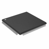
ADSP-2196MKSTZ-160 Analog Devices Inc, ADSP-2196MKSTZ-160 Datasheet - Page 20

ADSP-2196MKSTZ-160
Manufacturer Part Number
ADSP-2196MKSTZ-160
Description
IC DSP CONTROLLER 16BIT 144-LQFP
Manufacturer
Analog Devices Inc
Series
ADSP-21xxr
Type
Fixed Pointr
Datasheet
1.ADSP-2196MKSTZ-160.pdf
(68 pages)
Specifications of ADSP-2196MKSTZ-160
Interface
Host Interface, SPI, SSP, UART
Clock Rate
160MHz
Non-volatile Memory
ROM (48 kB)
On-chip Ram
40kB
Voltage - I/o
3.30V
Voltage - Core
2.50V
Operating Temperature
0°C ~ 70°C
Mounting Type
Surface Mount
Package / Case
144-LQFP
Device Core Size
16b
Format
Fixed Point
Clock Freq (max)
160MHz
Mips
160
Device Input Clock Speed
160MHz
Ram Size
40KB
Program Memory Size
48KB
Operating Supply Voltage (typ)
2.5/3.3V
Operating Supply Voltage (min)
2.37V
Operating Supply Voltage (max)
2.63/3.6V
Operating Temp Range
0C to 70C
Operating Temperature Classification
Commercial
Mounting
Surface Mount
Pin Count
144
Package Type
LQFP
Lead Free Status / RoHS Status
Lead free / RoHS Compliant
Available stocks
Company
Part Number
Manufacturer
Quantity
Price
Company:
Part Number:
ADSP-2196MKSTZ-160
Manufacturer:
Analog Devices Inc
Quantity:
10 000
ADSP-2196
Table 7. Pin Descriptions (Continued)
20
Pin
PF2
PF1
PF0
RD
WR
ACK
BMS
IOMS
MS3–0
BR
BG
BGH
HAD15–0
HA16
HACK_P
HRD
HWR
HACK
HALE
HCMS
HCIOMS
CLKIN
XTAL
BMODE1–0
OPMODE
CLKOUT
BYPASS
/SPI0SEL1
/MSEL2
/SPISS1
/MSEL1
/SPISS0
/MSEL0
This information applies to a product under development. Its characteristics and specifications are subject to change with-
out notice. Analog Devices assumes no obligation regarding future manufacturing unless otherwise agreed to in writing.
Type
I/O/T
I
I
I/O/T
I
I
I/O/T
I
I
O/T
O/T
I
O/T
O/T
O/T
I
O
O
I/O/T
I
I
I
I
O
I
I
I
I
O
I
I
O
I
Function
Programmable Flags 2/SPI0 Slave Select output 1 (when SPI0 enabled)/Multiplier Select 2
(during boot)
Programmable Flags 1/SPI1 Slave Select input (when SPI1 enabled)/Multiplier Select 1
(during boot)
Programmable Flags 0/SPI0 Slave Select input (when SPI0 enabled)/Multiplier Select 0
(during boot)
External Port Read Strobe
External Port Write Strobe
External Port Access Ready Acknowledge
External Port Boot Space Select
External Port IO Space Select
External Port Memory Space Selects
External Port Bus Request
External Port Bus Grant
External Port Bus Grant Hang
Host Port Multiplexed Address and Data Bus
Host Port MSB of Address Bus
Host Port ACK Polarity
Host Port Read Strobe
Host Port Write Strobe
Host Port Access Ready Acknowledge
Host Port Address Latch Strobe or Address Cycle Control
Host Port Internal Memory–Internal I/O Memory–Boot Memory Select
Host Port Internal I/O Memory Select
Clock Input/Oscillator input
Oscillator output
Boot Mode 1–0. The BMODE1 and BMODE0 pins have 85 k internal pull-up resistors.
Operating Mode. The OPMODE pin has a 85 k internal pull-up resistor.
Clock Output
Phase-Lock-Loop (PLL) Bypass mode. The BYPASS pin has a 85 k internal pull-up
resistor.
For current information contact Analog Devices at 800/262-5643
September 2001
REV. PrA


