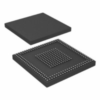
ADSP-BF527KBCZ-6C2 Analog Devices Inc, ADSP-BF527KBCZ-6C2 Datasheet - Page 38

ADSP-BF527KBCZ-6C2
Manufacturer Part Number
ADSP-BF527KBCZ-6C2
Description
IC DSP 16BIT 600MHZ 289CSPBGA
Manufacturer
Analog Devices Inc
Series
Blackfin®r
Type
Fixed Pointr
Datasheets
1.ADSP-BF531SBSTZ400.pdf
(12 pages)
2.ADSP-BF523BBCZ-5A.pdf
(88 pages)
3.ADSP-BF523KBCZ-5C2.pdf
(36 pages)
Specifications of ADSP-BF527KBCZ-6C2
Package / Case
289-CSPBGA
Interface
DMA, Ethernet, I²C, PPI, SPI, SPORT, UART, USB
Clock Rate
600MHz
Non-volatile Memory
ROM (32 kB)
On-chip Ram
132kB
Voltage - I/o
1.8V, 2.5V, 3.3V
Voltage - Core
1.10V
Operating Temperature
0°C ~ 70°C
Mounting Type
Surface Mount
Svhc
No SVHC (18-Jun-2010)
Cache On Chip L1/l2 Memory
48KB
Core Frequency Typ
600MHz
Dsp Type
Core
External Supported Memory
SDRAM, SRAM, FLASH, ROM
Interface Type
SPI, Parallel, 2 Wire
Rohs Compliant
Yes
Mmac
1200
No. Of Pins
289
Package
289CSP-BGA
Maximum Speed
600 MHz
Lead Free Status / RoHS Status
Lead free / RoHS Compliant
For Use With
ADZS-BF527-MPSKIT - BOARD EVAL MEDIA PLAYER BF527ADZS-BF527-EZLITE - BOARD EVAL ADSP-BF527
Lead Free Status / RoHS Status
Lead free / RoHS Compliant, Lead free / RoHS Compliant
Available stocks
Company
Part Number
Manufacturer
Quantity
Price
Company:
Part Number:
ADSP-BF527KBCZ-6C2
Manufacturer:
Analog Devices Inc
Quantity:
10 000
TIMING SPECIFICATIONS
Specifications are subject to change without notice.
Clock and Reset Timing
Table 31
the CCLK and SCLK timing specifications in
Table
not select core/peripheral clocks in excess of the processor's
maximum instruction rate.
Table 31. Clock and Reset Timing
1
2
3
4
5
Table 32. Power-Up Reset Timing
Parameter
Timing Requirements
t
Parameter
Timing Requirements
f
t
t
t
Switching Characteristic
t
Applies to PLL bypass mode and PLL nonbypass mode.
Combinations of the CLKIN frequency and the PLL clock multiplier must not exceed the allowed f
The t
If the DF bit in the PLL_CTL register is set, the minimum f
Applies after power-up sequence is complete. See
RST_IN_PWR
ADSP-BF522/ADSP-BF523/ADSP-BF524/ADSP-BF525/ADSP-BF526/ADSP-BF527
CKIN
CKINL
CKINH
WRST
BUFDLAY
Table 14 on Page 28
CKIN
17, combinations of CLKIN and clock multipliers must
period (see
and
RESET Deasserted after the V
Pins are Stable and Within Specification
Figure 9
CLKBUF
Figure
and
CLKIN
CLKIN Frequency (Commercial/ Industrial Models)
CLKIN Frequency (Automotive Models)
CLKIN Low Pulse
CLKIN High Pulse
RESET Asserted Pulse Width Low
CLKIN to CLKBUF Delay
Table 15 on Page 30
describe clock and reset operations. Per
9) equals 1/f
t
CKINL
CKIN
1
.
1
t
through
CKIN
DDINT
Table 32
t
CKINH
, V
Table 17 on Page
Table 12
DDEXT
CKIN
and
, V
specification is 24 MHz for commercial/industrial models and 28 MHz for automotive models.
Figure 10
5
Rev. B | Page 38 of 88 | May 2010
DDRTC
to
Figure 9. Clock and Reset Timing
t
WRST
, V
1, 2, 3, 4
30.
for power-up reset timing.
DDUSB
, V
DDMEM
1, 2, 3, 4
, V
DDOTP
Min
12
14
10
10
11 × t
, and CLKIN
VCO
CKIN
, f
CCLK
t
BUFDLAY
, and f
Min
3500 × t
SCLK
settings discussed in
CKIN
Max
50
50
10
Table 12 on Page 28
Max
t
BUFDLAY
through
Unit
ns
MHz
MHz
ns
ns
ns
Unit
ns


