ADSP-BF527KBCZ-6C2 Analog Devices Inc, ADSP-BF527KBCZ-6C2 Datasheet
ADSP-BF527KBCZ-6C2
Specifications of ADSP-BF527KBCZ-6C2
Available stocks


Related parts for ADSP-BF527KBCZ-6C2


ADSP-BF527KBCZ-6C2 Summary of contents
Page 1
... S Audio sampling rates: 8 kHz, 11.025 kHz, 12 kHz, 16 kHz, 22.05 kHz, 24 kHz, 32 kHz, 44.1 kHz, 48 kHz, 88.2 kHz, and 96 kHz PERIPHERALS See the published ADSP-BF52x processor data sheet for additional peripherals WATCHDOG TIMER OTP MEMORY RTC COUNTER PERIPHERAL ...
Page 2
... ADSP-BF522C/ADSP-BF523C/ADSP-BF524C/ADSP-BF525C/ADSP-BF526C/ADSP-BF527C TABLE OF CONTENTS Processor Features ................................................... 1 Embedded Codec Features ......................................... 1 Peripherals ............................................................. 1 Table of Contents ..................................................... 2 Revision History ...................................................... 2 General Description ................................................. 3 Codec Description ................................................ 3 ADC and DAC ..................................................... 4 ADC High-Pass and DAC De-Emphasis Filters ............ 4 Analog Audio Interfaces ......................................... 4 Stereo Line and Monaural Microphone Inputs .......... 4 Bypass and Sidetone Paths to Output ...................... 5 Line and Headphone Outputs ............................... 5 Digital Audio Interface ...
Page 3
... GENERAL DESCRIPTION This document describes the differences between the ADSP-BF52xC and the ADSP-BF52x standard Blackfin uct. Please refer to the published ADSP-BF52x data sheet for general description and specifications. This document only describes the differences from that data sheet. The ADSP-BF52xC processors add a low power, high quality ...
Page 4
... ADSP-BF522C/ADSP-BF523C/ADSP-BF524C/ADSP-BF525C/ADSP-BF526C/ADSP-BF527C To allow an external device to generate the central reference clock, apply the external clock signal directly through the XTI/ CODEC_MCLK input pin. In this configuration, the oscillator circuit of the codec can be powered down by using the OSCPD bit (Register R6, Bit D5) to reduce power consumption. ...
Page 5
... ADSP-BF522C/ADSP-BF523C/ADSP-BF524C/ADSP-BF525C/ADSP-BF526C/ADSP-BF527C 50kΩ R 10kΩ EXT 0dB/20dB/40dB GAIN BOOST MICIN AVDD VMID AGND Figure 3. Microphone Input to ADC The first gain stage is composed of a low noise operational amplifier set to an inverting configuration with integrated 50 kΩ feedback and 10 kΩ input resistors. The default micro- phone input signal gain ...
Page 6
... ADSP-BF522C/ADSP-BF523C/ADSP-BF524C/ADSP-BF525C/ADSP-BF526C/ADSP-BF527C The programmer can simultaneously load the volume control of both channels by writing to the LRHPBOTH (Register R2, Bit D8) and RLHPBOTH (Register R3, Bit D8) bits of the left- or right-channel DAC volume registers. The maximum output level of the headphone outputs is 1.0 V rms when AVDD and HPVDD = 3 suppress audi- ...
Page 7
... ADSP-BF522C/ADSP-BF523C/ADSP-BF524C/ADSP-BF525C/ADSP-BF526C/ADSP-BF527C LEFT CHANNEL ADCLRC/ DACLRC CODEC_BCLK ADCDAT DACDAT X = DON’T CARE. LEFT CHANNEL ADCLRC/ DACLRC CODEC_BCLK ADCDAT/ DACDAT X = DON’T CARE. Figure 9. Frame Sync/PCM Mode Audio Input (Submode 1) [Bit LRP = 0] LEFT CHANNEL ADCLRC/ DACLRC CODEC_BCLK ADCDAT/ DACDAT X = DON’T CARE. Figure 10. Frame Sync/PCM Mode Audio Input (Submode 2) [Bit LRP = 1] ...
Page 8
... ADSP-BF522C/ADSP-BF523C/ADSP-BF524C/ADSP-BF525C/ADSP-BF526C/ADSP-BF527C Recording Mode The digital audio interface sends the ADC digital filter data to the ADCDAT output pin for recording. The ADCDAT data stream multiplexes the left- and right-channel audio data in the time domain. The ADCLRC clock signal separates left- and right-channel digital audio frames on the ADCDAT lines. ...
Page 9
... ADSP-BF522C/ADSP-BF523C/ADSP-BF524C/ADSP-BF525C/ADSP-BF526C/ADSP-BF527C Normal Mode In normal mode, the codec supports digital audio sampling rates from 8 kHz to 96 kHz. Normal mode supports 256 × f 384 × f based clocks. To select the desired sampling rate, the S programmer must set the appropriate sampling rate register in Table 1. Sampling Rate Lookup Table, Normal Mode (USB Disabled) ...
Page 10
... ADSP-BF522C/ADSP-BF523C/ADSP-BF524C/ADSP-BF525C/ADSP-BF526C/ADSP-BF527C USB Mode In USB mode, the codec supports digital audio sampling rates from 8 kHz to 96 kHz. USB mode is enabled on the codec to support the common universal serial bus (USB) clock rate of Table 2. Sampling Rate Lookup Table, USB Mode (USB Enabled) CODEC_MCLK CODEC_MCLK ...
Page 11
... ADSP-BF522C/ADSP-BF523C/ADSP-BF524C/ADSP-BF525C/ADSP-BF526C/ADSP-BF527C SOFTWARE CONTROL INTERFACE The software control interface provides access to the programmer-selectable control registers and can operate with a 2-wire (TWI) or 3-wire (SPI) interface, depending on the setting of the CMODE pin. If the CMODE pin is set to 0, the 2-wire interface is selected the 3-wire interface is selected. ...
Page 12
... ADSP-BF522C/ADSP-BF523C/ADSP-BF524C/ADSP-BF525C/ADSP-BF526C/ADSP-BF527C CODEC PIN DESCRIPTIONS Table 3 shows the signals added to the ADSP-BF52xC processor for the embedded codec. Please refer to the published ADSP-BF52x data sheet for descriptions of other signals for the processor. Table 3. Codec Pin Descriptions Pin Name Type Function Codec CODEC_CLKOUT O Codec Clock Output ...
Page 13
... ADSP-BF522C/ADSP-BF523C/ADSP-BF524C/ADSP-BF525C/ADSP-BF526C/ADSP-BF527C Figure 14 on Page 13 and Figure 15 on Page 14 tive external connections for SPI or TWI control of the ADSP-BF52xC codec. The figures are the same except for the shaded area in each AVDD SPI describe alterna- ADSP-BF52XC XTI/CODEC_MCLK XTO DACLRC DACDAT ADCDAT ADCLRC CODEC_BCLK ...
Page 14
... ADSP-BF522C/ADSP-BF523C/ADSP-BF524C/ADSP-BF525C/ADSP-BF526C/ADSP-BF527C AVDD SEE VERSION 2.1 OF THE I2C SPECIFICATION R R FOR THE PROPER RESISTOR VALUE AVDD 10 K: TWI ADSP-BF52XC XTI/CODEC_MCLK XTO DACLRC DACDAT ADCDAT ADCLRC CODEC_BCLK BLACKFIN PROCESSOR RSCLKx RFSx DRxPRI DTxPRI TFSx MOSI SCK SDA SCL CSCL CSDA CSB CMODE Figure 15. Recommended Application Circuit Using TWI Control Rev ...
Page 15
... ADSP-BF522C/ADSP-BF523C/ADSP-BF524C/ADSP-BF525C/ADSP-BF526C/ADSP-BF527C REGISTER DETAILS Register Address Register 0 Left-Channel ADC 0x00 Input Volume on Page 16 Register 1 Right-Channel ADC 0x01 Input Volume on Page 17 Register 2 Left-Channel DAC 0x02 Volume on Page 17 Register 3 Right-Channel DAC 0x03 Volume on Page 18 Register 4 Analog Audio Path 0x04 on Page 18 Register 5 Digital Audio Path ...
Page 16
... ADSP-BF522C/ADSP-BF523C/ADSP-BF524C/ADSP-BF525C/ADSP-BF526C/ADSP-BF527C BIT DESCRIPTIONS Table 4 through Table 14 on Page 20 describe each bit in the control registers. Table 4. Register 0 Left-Channel ADC Input Volume Bit Name Bits Description LRINBOTH B8 Left-to-right line input ADC data load control LINMUTE B7 Left-channel input mute LINVOL B[5:0] Left-channel PGA volume control ...
Page 17
... ADSP-BF522C/ADSP-BF523C/ADSP-BF524C/ADSP-BF525C/ADSP-BF526C/ADSP-BF527C Table 5. Register 1 Right-Channel ADC Input Volume Bit Name Bits Description RLINBOTH B8 Right-to-left line input ADC data load control RINMUTE B7 Right-channel input mute RINVOL B[5:0] Right-channel PGA volume control Table 6. Register 2 Left-Channel DAC Volume Bit Name Bits Description LRHPBOTH B8 Left-to-right headphone volume ...
Page 18
... ADSP-BF522C/ADSP-BF523C/ADSP-BF524C/ADSP-BF525C/ADSP-BF526C/ADSP-BF527C Table 7. Register 3 Right-Channel DAC Volume Bit Name Bits Description RLHPBOTH B8 Right-to-left headphone volume load control RZCEN B7 Right-channel zero cross detect enable RHPVOL [6:0] B[6:0] Right-channel headphone volume control Table 8. Register 4 Analog Audio Path Bit Name Bits Description MICBOOST2 B8 Additional microphone amplifier gain booster control ...
Page 19
... ADSP-BF522C/ADSP-BF523C/ADSP-BF524C/ADSP-BF525C/ADSP-BF526C/ADSP-BF527C Table 9. Register 5 Digital Audio Path Bit Name Bits Description HPOR B4 Store dc offset when high-pass filter is disabled DACMU B3 DAC digital mute DEEMPH[1:0] B[2:1] De-emphasis control ADCHPD B0 ADC high-pass filter control Table 10. Register 6 Power Management Bit Name Bits Description POWEROFF B7 Whole chip power-down control ...
Page 20
... ADSP-BF522C/ADSP-BF523C/ADSP-BF524C/ADSP-BF525C/ADSP-BF526C/ADSP-BF527C Table 11. Register 7 Digital Audio I/F Bit Name Bits Description BCLKINV B7 CODEC_BCLK inversion control MS B6 Master mode enable LRSWAP B5 Swap DAC data control LRP B4 Polarity control for clocks in right-justified, left-justified, and I WL [1:0] B[3:2] Data-word length control FORMAT [1:0] B[1:0] Digital audio input format control Table 12 ...
Page 21
... T = 25°C, AVDD = VDDEXT = 3.3 V, HPVDD = 3.3 V, Ambient 1 kHz signal kHz, PGA gain = 0 dB, 24-bit audio data, S unless otherwise noted. OPERATING CONDITIONS See operating conditions in the published ADSP-BF52xC data sheet. Parameter 1 AVDD HPVDD 1 Note that AVDD must equal HPVDD. CODEC ELECTRICAL CHARACTERISTICS ...
Page 22
... ADSP-BF522C/ADSP-BF523C/ADSP-BF524C/ADSP-BF525C/ADSP-BF526C/ADSP-BF527C Parameter Line Output DAC Full-Scale Output Signal-to-Noise Ratio (A-Weighted) THD + N Power Supply Rejection Ratio Channel Separation Headphone Output Full-Scale Output Voltage Maximum Output Power Signal-to-Noise Ratio (A-Weighted) THD + N Power Supply Rejection Ratio Mute Attenuation LIne Input To Line Output Full-Scale Output Voltage ...
Page 23
... ESD. Therefore, proper ESD precautions should be taken to avoid performance degradation or loss of functionality. PACKAGE INFORMATION The information presented in Figure 17 details about the package branding for the ADSP-BF52xC pro- cessor. For a complete listing of product availability, see Ordering Guide on Page 36. ADSP-BF527KBCZ6C2X tppZccc vvvvvv ...
Page 24
... ADSP-BF522C/ADSP-BF523C/ADSP-BF524C/ADSP-BF525C/ADSP-BF526C/ADSP-BF527C POWER CONSUMPTION These current consumption values are for the codec alone. Please refer to the published ADSP-BF52x processor data sheet for the additional current consumption of the Blackfin processor. Table 16. Power Consumption Mode Record and Playback 0 Playback Only Oscillator Enabled 0 External Clock ...
Page 25
... ADSP-BF522C/ADSP-BF523C/ADSP-BF524C/ADSP-BF525C/ADSP-BF526C/ADSP-BF527C TIMING SPECIFICATIONS TWI Timing Table 17. TWI Timing Parameter t Start condition setup time SCS t Start condition hold time SCH t CSCL pulse width high PH t CSCL pulse width low PL f CSCL frequency SCL t Data setup time DS t Data hold time DH t CSDA and CSCL rise time ...
Page 26
... ADSP-BF522C/ADSP-BF523C/ADSP-BF524C/ADSP-BF525C/ADSP-BF526C/ADSP-BF527C SPI Timing Table 18. SPI Timing Parameter t CSDA to CSCL setup time DSU t CSCL to CSDA hold time DHO t CSCL pulse width high SCH t CSCL pulse width low SCL t CSCL rising edge to CSB rising edge SCS t CSB rising to CSCL rising CSS t CSB pulse width high ...
Page 27
... ADSP-BF522C/ADSP-BF523C/ADSP-BF524C/ADSP-BF525C/ADSP-BF526C/ADSP-BF527C Digital Audio Interface Slave Mode Timing Table 19. Digital Audio Interface Slave Mode Timing Parameter t DACDAT setup time from CODEC_BCLK rising edge DS t DACDAT hold time from CODEC_BCLK rising edge DH t ADCLRC/DACLRC setup time to CODEC_BCLK rising edge LRSU t ADCLRC/DACLRC hold time to CODEC_BCLK rising edge ...
Page 28
... ADSP-BF522C/ADSP-BF523C/ADSP-BF524C/ADSP-BF525C/ADSP-BF526C/ADSP-BF527C Digital Audio Interface Master Mode Timing Table 20. Digital Audio Interface Master Mode Timing Parameter t DACDAT setup time to CODEC_BCLK rising edge DST t DACDAT hold time to CODEC_BCLK rising edge DHT t ADCLRC/DACLRC propagation delay from CODEC_BCLK falling edge DL t ADCDAT propagation delay from CODEC_BCLK falling edge ...
Page 29
... ADSP-BF522C/ADSP-BF523C/ADSP-BF524C/ADSP-BF525C/ADSP-BF526C/ADSP-BF527C System Clock Timing Table 21. System Clock Timing Parameter t XTI/CODEC_MCLK system clock cycle time XTIY t XTI/CODEC_MCLK duty cycle MCLKDS t XTI/CODEC_MCLK system clock pulse width high XTIH t XTI/CODEC_MCLK system clock pulse width low XTIL t CODEC_CLKOUT propagation delay from XTI/CODEC_MCLK falling edge COP ...
Page 30
... ADSP-BF522C/ADSP-BF523C/ADSP-BF524C/ADSP-BF525C/ADSP-BF526C/ADSP-BF527C Digital Filter Characteristics Table 22. Digital Filter Characteristics Parameter Conditions ADC FILTER Pass Band ±0.04 dB –6 dB Pass Band Ripple Stop Band Stop Band Attenuation f > 0.567 × f High-Pass Filter Corner Frequency –3 dB –0.5 dB –0.1 dB DAC FILTER Pass Band ±0.04 dB –6 dB Pass Band Ripple ...
Page 31
... ADSP-BF522C/ADSP-BF523C/ADSP-BF524C/ADSP-BF525C/ADSP-BF526C/ADSP-BF527C 0 –10 –20 –30 –40 –50 –60 –70 –80 –90 –100 0 0.25 0.50 0.75 1.00 1.25 f FREQUENCY ( ) S Figure 25. DAC Digital Filter Frequency Response, Sampling Rate = 48 kHz 0.05 0.04 0.03 0.02 0.01 0 −0.01 −0.02 −0.03 −0.04 −0.05 0 0.05 0.10 0.15 0.20 0.25 0.30 0.35 0.40 0.45 0.50 ...
Page 32
... FREQUENCY (kHz) Figure 32. De-Emphasis Error, Sampling Rate = 48 kHz 289-BALL CSP_BGA BALL ASSIGNMENT Signals added or changed to the ADSP-BF52xC processor for the embedded codec are shown in refer to the published ADSP-BF52x processor data sheet for descriptions of additional signals for the processor. Table 23. 289-Ball CSP_BGA Ball Assignment ...
Page 33
... ADSP-BF52xC processor ball configuration. A1 BALL PAD CORNER KEY: V GND DDINT V I/O V DDEXT DDMEM BALLS THAT HAVE CHANGED USAGE ON THE ADSP-BF522C/523C/524C/525C/526C/527C: CODEC I/O AVDD HPVDD HPGND AGND TOP VIEW Figure 33. ADSP-BF52xC Processor Ball Configuration (Top View) Rev Page March 2010 ...
Page 34
... ADSP-BF52xC proces- sor ball configuration KEY: V GND DDINT V I/O DDEXT BALLS THAT HAVE CHANGED USAGE ON THE ADSP-BF522C/523C/524C/525C/526C/527C: CODEC I/O AVDD HPVDD HPGND AGND BOTTOM VIEW V DDMEM Figure 34. ADSP-BF52xC Processor Ball Configuration (Bottom View) Rev Page March 2010 A1 BALL PAD CORNER ...
Page 35
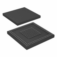
... ADSP-BF522C/ADSP-BF523C/ADSP-BF524C/ADSP-BF525C/ADSP-BF526C/ADSP-BF527C OUTLINE DIMENSIONS Dimensions in Figure 35, 289-Ball CSP_BGA (BC-289-2) shown in millimeters. 12.00 BSC SQ A1 BALL PAD CORNER TOP VIEW 1.40 1.26 1.11 SIDE VIEW NOTES 1. DIMENSIONS ARE IN MILLIMETERS. 2. COMPLIES WITH JEDEC REGISTERED OUTLINE MO-195, VARIATION AJ AND EXCEPTION TO PACKAGE HEIGHT AND BALL HEIGHT. ...
Page 36
... ADSP-BF526KBCZ-3C2 0°C to +70°C ADSP-BF526KBCZ-4C2 0°C to +70°C ADSP-BF527KBCZ-5C2 0°C to +70°C ADSP-BF527KBCZ-6C2 0°C to +70° RoHS Compliant Part. 2 Referenced temperature is ambient temperature. The ambient temperature is not a specification. Please see specification which is the only temperature specification. ©2010 Analog Devices, Inc. All rights reserved. Trademarks and registered trademarks are the property of their respective owners ...