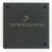
DSPB56362AG120 Freescale Semiconductor, DSPB56362AG120 Datasheet - Page 90

DSPB56362AG120
Manufacturer Part Number
DSPB56362AG120
Description
IC DSP 24BIT AUD 120MHZ 144-LQFP
Manufacturer
Freescale Semiconductor
Series
Symphony™r
Type
Audio Processorr
Datasheet
1.DSPB56362AG120.pdf
(152 pages)
Specifications of DSPB56362AG120
Interface
Host Interface, I²C, SAI, SPI
Clock Rate
120MHz
Non-volatile Memory
ROM (126 kB)
On-chip Ram
42kB
Voltage - I/o
3.30V
Voltage - Core
3.30V
Operating Temperature
-40°C ~ 85°C
Mounting Type
Surface Mount
Package / Case
144-LQFP
Device Core Size
24b
Architecture
Modified Harvard
Format
Fixed Point
Clock Freq (max)
120MHz
Mips
120
Device Input Clock Speed
120MHz
Ram Size
42KB
Program Memory Size
90KB
Operating Supply Voltage (typ)
3.3V
Operating Supply Voltage (min)
3.14V
Operating Supply Voltage (max)
3.46V
Operating Temp Range
-40C to 105C
Operating Temperature Classification
Industrial
Mounting
Surface Mount
Pin Count
144
Package Type
LQFP
Product
DSPs
Data Bus Width
24 bit
Processor Series
DSP563xx
Core
56000
Numeric And Arithmetic Format
Fixed-Point
Instruction Set Architecture
Modified Harvard
Device Million Instructions Per Second
120 MIPS
Maximum Clock Frequency
120 MHz
Program Memory Type
Flash
Data Ram Size
42 KB
Operating Supply Voltage
3.3 V
Maximum Operating Temperature
+ 105 C
Mounting Style
SMD/SMT
Interface Type
SPI, I2C, ESAI, SHI
Minimum Operating Temperature
- 40 C
Lead Free Status / RoHS Status
Lead free / RoHS Compliant
Available stocks
Company
Part Number
Manufacturer
Quantity
Price
Company:
Part Number:
DSPB56362AG120
Manufacturer:
FSC
Quantity:
12 000
Company:
Part Number:
DSPB56362AG120
Manufacturer:
FREESCA
Quantity:
273
Company:
Part Number:
DSPB56362AG120
Manufacturer:
Freescale Semiconductor
Quantity:
10 000
Part Number:
DSPB56362AG120
Manufacturer:
N/A
Quantity:
20 000
Enhanced Serial Audio Interface Timing
1
2
3
4
5
6
7
3-64
458 FST input (wl) to data out enable from high
459 FST input (wl) to transmitter drive enable
460 FST input (wl) setup time before TXC falling
461 FST input hold time after TXC falling edge
462 Flag output valid after TXC rising edge
463 HCKR/HCKT clock cycle
464 HCKT input rising edge to TXC output
465 HCKR input rising edge to RXC output
No.
V
i ck = internal clock
x ck = external clock
i ck a = internal clock, asynchronous mode (asynchronous implies that TXC and RXC are two different clocks)
i ck s = internal clock, synchronous mode (synchronous implies that TXC and RXC are the same clock)
bl = bit length
wl = word length
wr = word length relative
TXC(SCKT pin) = transmit clock
RXC(SCKR pin) = receive clock
FST(FST pin) = transmit frame sync
FSR(FSR pin) = receive frame sync
HCKT(HCKT pin) = transmit high frequency clock
HCKR(HCKR pin) = receive high frequency clock
For the internal clock, the clock cycle at the pin is defined by Icyc and the ESAI control registers.
The word-relative frame sync signal waveform relative to the clock operates in the same manner as the bit-length frame sync
signal waveform, but spreads from one serial clock before first bit clock (same as bit length frame sync signal), until the one
before last bit clock of the first word in frame.
Periodically sampled and not 100% tested.
CC
impedance
assertion
edge
= 3.3 V ± 0.16 V; T
Characteristics
Table 3-24 Enhanced Serial Audio Interface Timing (continued)
J
= 0°C to +100°C, C
1
,
2, 3
DSP56362 Technical Data, Rev. 4
L
= 50 pF
Symbol
—
—
—
—
—
—
—
—
Expression
—
—
—
—
—
—
—
—
21.0
40.0
Min
2.0
4.0
0.0
—
—
—
—
—
—
100 MHz
Max
27.0
31.0
32.0
18.0
27.5
27.5
—
—
—
—
—
Freescale Semiconductor
Condition
x ck
x ck
x ck
i ck
i ck
i ck
—
—
4
Unit
ns
ns
ns
ns
ns
ns
ns
ns


