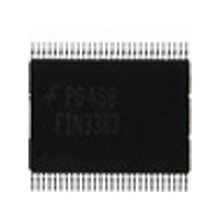
FIN3386MTD Fairchild Semiconductor, FIN3386MTD Datasheet - Page 12

FIN3386MTD
Manufacturer Part Number
FIN3386MTD
Description
Manufacturer
Fairchild Semiconductor
Datasheet
1.FIN3386MTD.pdf
(21 pages)
Specifications of FIN3386MTD
Number Of Elements
4
Number Of Receivers
4
Number Of Drivers
28
Input Type
CMOS/TTL
Operating Supply Voltage (typ)
3.3V
Differential Input High Threshold Voltage
100mV
Diff. Input Low Threshold Volt
-100mV
Output Type
Deserializer
Operating Supply Voltage (min)
3V
Operating Supply Voltage (max)
3.6V
Operating Temp Range
-10C to 70C
Operating Temperature Classification
Commercial
Mounting
Surface Mount
Pin Count
56
Package Type
TSSOP
Lead Free Status / Rohs Status
Compliant
© 2003 Fairchild Semiconductor Corporation
FIN3383/3384/3385/3386 • Rev. 1.0.4
Receiver AC Electrical Characteristics (66MHz)
Notes:
18. For the receiver with falling-edge strobe, the definition of setup/hold time is slightly different from the one with
19. Total channel latency from serializer to deserializer is (T + t
20. Receiver skew margin is defined as the valid sampling window after considering potential setup/hold time and
Symbol
t
t
t
t
t
t
t
t
t
t
t
t
t
t
t
t
t
t
t
t
t
t
t
t
t
t
t
t
t
RSPB0
RSPB1
RSPB2
RSPB3
RSPB4
RSPB5
RSPB6
RSPB0
RSPB1
RSPB2
RSPB3
RSPB4
RSPB5
RSPB6
RPLLS
RCOP
RCOL
RCOH
RSRC
RHRC
RCOL
RCOH
RSRC
RHRC
ROLH
ROHL
RCCD
RPDD
RSKM
rising-edge strobe. The clock reference point is the time when the clock falling edge passes through 2V. For
hold time tRHRC, the clock reference point is the time when falling edge passes through +0.8V.
minimum / maximum bit position.
Receiver Clock Output (RxCLKOut)
Period
RxCLKOut LOW Time
RxCLKOut HIGH Time
RxOUT Valid Prior to RxCLKOut
RxOUT Valid After RxCLKOut
RxCLKOut LOW Time
RxCLKOut HIGH Time
RxOUT Valid Prior to RxCLKOut
RxOUT Valid After RxCLKOut
Output Rise Time (20% to 80%)
Output Fall Time (20% to 80%)
Receiver Clock Input to Clock Output
Delay
Receiver Power-Down Delay
Receiver Input Strobe Position of Bit 0
Receiver Input Strobe Position of Bit 1
Receiver Input Strobe Position of Bit 2
Receiver Input Strobe Position of Bit 3
Receiver Input Strobe Position of Bit 4
Receiver Input Strobe Position of Bit 5
Receiver Input Strobe Position of Bit 6
Receiver Input Strobe Position of Bit 0
Receiver Input Strobe Position of Bit 1
Receiver Input Strobe Position of Bit 2
Receiver Input Strobe Position of Bit 3
Receiver Input Strobe Position of Bit 4
Receiver Input Strobe Position of Bit 5
Receiver Input Strobe Position of Bit 6
RxIn Skew Margin
Receiver Phase Lock Loop Set Time
(19)
Parameter
(20)
12
Figure 12
Figure 12
Rising Edge Strobe
f=40MHz
Figure 12
Rising Edge
Strobe
C
Figure 12
Figure 14
T
V
Figure 17
Figure 21
f=40MHz
Figure 21
f=66MHz
f=40MHz, Figure 21
f=66MHz, Figure 21
Figure 15
A
L
CC
=25°C and
=8pF
=3.3v
Conditions
(18)
CCD
(18)
f=66MHz
) (2•T + t
RCCD
). There is the clock period.
Min.
10.0
10.0
1.00
8.10
11.6
15.1
18.8
22.5
11.7
13.9
490
400
6.5
6.0
5.0
5.0
4.5
4.0
3.5
4.5
0.7
2.9
5.1
7.3
9.5
15
Typ.
11.0
12.2
11.6
11.6
1.40
8.50
11.9
15.6
19.2
22.9
12.1
14.3
6.3
7.6
7.3
6.3
2.0
1.8
5.0
5.0
1.1
3.3
5.5
7.7
9.9
T
Max.
2.15
9.15
12.6
16.3
19.9
23.6
10.2
12.4
14.6
10.0
9.0
9.0
5.0
5.0
7.5
1.0
5.8
1.4
3.6
5.8
8.0
50
www.fairchildsemi.com
Units
ms
ns
ns
ns
ns
ns
µs
ns
ns
ps


