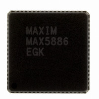
MAX5886EGK+D Maxim Integrated Products, MAX5886EGK+D Datasheet - Page 12

MAX5886EGK+D
Manufacturer Part Number
MAX5886EGK+D
Description
IC DAC 12BIT 3.3V 500MSPS 68-QFN
Manufacturer
Maxim Integrated Products
Datasheet
1.MAX5886EGKD.pdf
(18 pages)
Specifications of MAX5886EGK+D
Settling Time
11ns
Number Of Bits
12
Data Interface
Parallel
Number Of Converters
1
Voltage Supply Source
Analog and Digital
Power Dissipation (max)
130mW
Operating Temperature
-40°C ~ 85°C
Mounting Type
Surface Mount
Package / Case
68-QFN Exposed Pad
Number Of Dac Outputs
1
Conversion Rate
500 MSPs
Resolution
12 bit
Interface Type
Serial
Supply Voltage (max)
3.465 V
Supply Voltage (min)
3.135 V
Maximum Operating Temperature
+ 85 C
Mounting Style
SMD/SMT
Maximum Power Dissipation
3333 mW
Minimum Operating Temperature
- 40 C
Supply Current
6.4 mA
Lead Free Status / RoHS Status
Lead free / RoHS Compliant
If a single-ended unipolar output is desirable, IOUTP
should be selected as the output, with IOUTN ground-
ed. However, driving the MAX5886 single ended is not
recommended since additional noise is added (from
the ground plane) in such configurations.
The distortion performance of the DAC depends on the
load impedance. The MAX5886 is optimized for a 50Ω
double termination. It can be used with a transformer
output as shown in Figure 7 or just one 50Ω resistor
from each output to ground and one 50Ω resistor
between the outputs. This produces a full-scale output
power of up to 0dBm depending on the output current
setting. Higher termination impedance can be used at
the cost of degraded distortion performance and
increased output noise voltage.
3.3V, 12-Bit, 500Msps High Dynamic
Performance DAC with Differential LVDS Inputs
Figure 7. Differential to Single-Ended Conversion Using a Wideband RF Transformer
Figure 8. MAX5886 Differential Output Configuration
12
12
B0–B11
______________________________________________________________________________________
AGND
AV
DD
12
MAX5886
B0–B11
DGND
DV
DD
CLKGND
VCLK
AGND
AV
DD
MAX5886
DGND
DV
IOUTN
IOUTP
DD
CLKGND
VCLK
50Ω
100Ω
50Ω
IOUTN
IOUTP
OUTP
OUTN
50Ω
100Ω
50Ω
The transmitter sections of BTS applications serving
CDMA and W-CDMA architectures must generate carri-
ers with minimal coupling of carrier energy into the
adjacent channels. Similar to the GSM/EDGE model
(see the Multitone Testing for GSM/EDGE Applications
section), a transmit mask (Tx mask) exists for this appli-
cation. The spread-spectrum modulation function
applied to the carrier frequency generates a spectral
response, which is uniform over a given bandwidth (up
to 4MHz) for a W-CDMA-modulated carrier.
A dominant specification is ACLR, a parameter which
reflects the ratio of the power in the desired carrier
band to the power in an adjacent carrier band. The
specification covers the first two adjacent bands, and is
measured on both sides of the desired carrier.
According to the transmit mask for CDMA and W-CDMA
architectures, the power ratio of the integrated carrier
channel energy to the integrated adjacent channel
energy must be >45dB for the first adjacent carrier slot
(ACLR 1) and >50dB for the second adjacent carrier
slot (ACLR 2). This specification applies to the output of
the entire transmitter signal chain. The requirement for
only the DAC block of the transmitter must be tighter,
with a typical margin of >15dB, requiring the DAC’s
ACLR 1 to be better than 60dB. Adjacent channel leak-
age is caused by a single spread-spectrum carrier,
which generates intermodulation (IM) products
T1, 1:1
Adjacent Channel Leakage Power Ratio
T2, 1:1
PERFORMS THE DIFFERENTIAL TO
WIDEBAND RF TRANSFORMER T2
SINGLE-ENDED CONVERSION.
(ACLR) Testing for CDMA- and
W-CDMA-Based Base Station
V
OUT
Transceiver Systems (BTS)
, SINGLE ENDED


